R
Platform Flash In-System Programmable Configuration PROMs
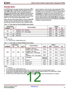
Standby Mode
The PROM enters a low-power standby mode whenever CE is
deasserted (High). In standby mode, the address counter is
reset, CEO is driven High, and the remaining outputs are
placed in a high-impedance state regardless of the state of the
OE/RESET input. For the device to remain in the low-power
standby mode, the JTAG pins TMS, TDI, and TDO must not be
pulled Low, and TCK must be stopped (High or Low).
pull-up resistor is used, but refer to the appropriate FPGA
data sheet for the recommended DONE pin pull-up value. If
the DONE circuit is connected to an LED to indicate FPGA
configuration is complete, and is also connected to the
PROM CE pin to enable low-power standby mode, then an
external buffer should be used to drive the LED circuit to
ensure valid transitions on the PROM’s CE pin. If low-power
standby mode is not required for the PROM, then the CE pin
should be connected to ground.
When using the FPGA DONE signal to drive the PROM CE
pin High to reduce standby power after configuration, an
external pull-up resistor should be used. Typically a 330Ω
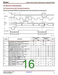
Table 10: Truth Table for XCFxxS PROM Control Inputs
Control Inputs
Outputs
Internal Address
If address < TC(2) : increment
OE/RESET
CE
DATA
Active
High-Z
High-Z
High-Z
CEO
High
Low
ICC
Active
High
Low
If address = TC(2) : don't change
Held reset
Reduced
Active
Low
X(1)
Low
High
High
High
Held reset
Standby
Notes:
1. X = don’t care.
2. TC = Terminal Count = highest address value.
Table 11: Truth Table for XCFxxP PROM Control Inputs
Control Inputs
Outputs
Internal Address
OE/RESET
CE
CF
BUSY(5)
DATA
CEO
CLKOUT
ICC
If address < TC(2) and
Active
High
Active
Active
address < EA(3) : increment
If address < TC(2) and
High
Low
High
Low
High-Z
High-Z
High
Low
High
High-Z
High-Z
Active
Reduced
Reduced
Active
address = EA(3) : don't change
Else
If address = TC(2) : don't change
Unchanged
Active and
Unchanged
High
Low
High
High
High
Low
X
Low
Low
High
↑
X
X
X(1)
X
Reset(4)
Active
High-Z
High-Z
High
High
High
Active
High-Z
High-Z
Active
Active
Held reset(4)
Held reset(4)
X
Standby
Notes:
1. X = don’t care.
2. TC = Terminal Count = highest address value.
3. For the XCFxxP with Design Revisioning enabled, EA = end address (last address in the selected design revision).
4. For the XCFxxP with Design Revisioning enabled, Reset = address reset to the beginning address of the selected bank. If Design
Revisioning is not enabled, then Reset = address reset to address 0.
5. The BUSY input is only enabled when the XCFxxP is programmed for parallel data output and decompression is not enabled.
DS123 (v2.18) May 19, 2010
www.xilinx.com
Product Specification
12

 XILINX [ XILINX, INC ]