R
Platform Flash In-System Programmable Configuration PROMs
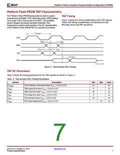
X-Ref Target - Figure 5
PROM 0
PROM 0
PROM 0
PROM 0
PROM 0
REV 0
REV 0
REV 0
(8 Mbits)
(8 Mbits)
(8 Mbits)
REV 0
(16 Mbits)
REV 1
REV 1
(8 Mbits)
(8 Mbits)
REV 0
(32 Mbits)
REV 1
REV 2
(8 Mbits)
(24 Mbits)
REV 2
REV 1
(16 Mbits)
(16 Mbits)
REV 3
(8 Mbits)
4 Design Revisions 3 Design Revisions
2 Design Revisions
1 Design Revision
PROM 0
(a) Design Revision storage examples for a single XCF32P PROM
PROM 0
PROM 0
PROM 0
PROM 0
REV 0
REV 0
REV 0
(16 Mbits)
(16 Mbits)
(16 Mbits)
REV 0
REV 0
(32 Mbits)
(32 Mbits)
REV 1
REV 1
REV 1
(16 Mbits)
(16 Mbits)
(16 Mbits)
PROM 1
PROM 1
PROM 1
PROM 1
PROM 1
REV 2
(16 Mbits)
REV 2
REV 1
REV 1
REV 0
(32 Mbits)
(32 Mbits)
(32 Mbits)
(32 Mbits)
REV 3
(16 Mbits)
4 Design Revisions 3 Design Revisions
2 Design Revisions
1 Design Revision
ds123_20_102103
(b) Design Revision storage examples spanning two XCF32P PROMs
Figure 5: Design Revision Storage Examples
Initiating FPGA Configuration
The options for initiating FPGA configuration via the
Platform Flash PROM include:
When using the XCFxxP Platform Flash PROM with design
revisioning enabled, the CF pin should always be connected
to the PROGRAM_B pin on the FPGA to ensure that the
current design revision selection is sampled when the
FPGA is reset. The XCFxxP PROM samples the current
design revision selection from the external REV_SEL pins
or the internal programmable Revision Select bits on the
rising edge of CF. When the JTAG CONFIG command is
executed, the XCFxxP samples the new design revision
selection before initiating the FPGA configuration
sequence. When using the XCFxxP Platform Flash PROM
without design revisioning, if the CF pin is not connected to
the FPGA PROGRAM_B pin, then the XCFxxP CF pin must
be tied High.
•
•
Automatic configuration on power up
Applying an external pulse to the FPGA PROGRAM_B
pin
•
Applying the JTAG CONFIG instruction to the PROM
Following the FPGA’s power-on sequence or the assertion
of the PROGRAM_B pin, the FPGA’s configuration memory
is cleared, the configuration mode is selected, and the
FPGA is ready to accept a new configuration bitstream. The
FPGA’s PROGRAM_B pin can be controlled by an external
source, or alternatively, the Platform Flash PROMs
incorporate a CF pin that can be tied to the FPGA’s
PROGRAM_B pin. Executing the CONFIG instruction
through JTAG pulses the CF output Low once for
300-500 ns, resetting the FPGA and initiating configuration.
The iMPACT software can issue the JTAG CONFIG
command to initiate FPGA configuration by setting the
“Load FPGA” option.
DS123 (v2.18) May 19, 2010
www.xilinx.com
Product Specification
10

 XILINX [ XILINX, INC ]