R
Platform Flash In-System Programmable Configuration PROMs
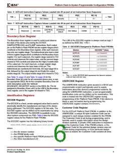
Table 6: XCFxxS Instruction Capture Values Loaded into IR as part of an Instruction Scan Sequence
IR[7:5]
IR[4]
IR[3]
IR[2]
IR[1:0]
TDI →
→ TDO
→ TDO
Reserved
ISC Status
Security
0
0 1
Table 7: XCFxxP Instruction Capture Values Loaded into IR as part of an Instruction Scan Sequence
IR[15:9]
IR[8:7]
IR[6:5]
IR[4]
IR[3]
IR[2]
IR[1:0]
TDI →
ER/PROG
Error
ER/PROG
Status
Reserved
ISC Error
ISC Status
DONE
0 1
Boundary-Scan Register
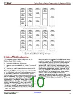
The Boundary-Scan register is used to control and observe
the state of the device pins during the EXTEST,
The LSB of the IDCODE register is always read as logic 1
as defined by IEEE Std. 1149.1.
SAMPLE/PRELOAD, and CLAMP instructions. Each output
pin on the Platform Flash PROM has two register stages which
contribute to the Boundary-Scan register, while each input pin
has only one register stage. The bidirectional pins have a total
of three register stages which contribute to the Boundary-Scan
register. For each output pin, the register stage nearest to TDI
controls and observes the output state, and the second stage
closest to TDO controls and observes the High-Z enable state
of the output pin. For each input pin, a single register stage
controls and observes the input state of the pin. The
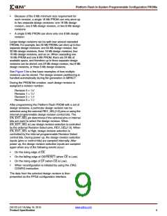
Table 8: IDCODES Assigned to Platform Flash PROMs
Device
XCF01S
XCF02S
XCF04S
XCF08P
XCF16P
XCF32P
IDCODE(1) (hex)
<v>5044093
<v>5045093
<v>5046093
<v>5057093
<v>5058093
<v>5059093
bidirectional pin combines the three bits, the input stage bit is
first, followed by the output stage bit and finally the output
enable stage bit. The output enable stage bit is closest to TDO.
Notes:
1. The <v> in the IDCODE field represents the device’s revision
code (in hex) and can vary.
See Table 12, page 24 and Table 13, page 26 for the
Boundary-Scan bit order for all connected device pins, or see
the appropriate BSDL file for the complete Boundary-Scan bit
order description under the “attribute
BOUNDARY_REGISTER” section in the BSDL file. The bit
assigned to Boundary-Scan cell 0 is the LSB in the Boundary-
Scan register, and is the register bit closest to TDO.
USERCODE Register
The USERCODE instruction gives access to a 32-bit user
programmable scratch pad typically used to supply
information about the device's programmed contents. By
using the USERCODE instruction, a user-programmable
identification code can be shifted out for examination. This
code is loaded into the USERCODE register during
programming of the Platform Flash PROM. If the device is
blank or was not loaded during programming, the
USERCODE register contains FFFFFFFFh.
Identification Registers
IDCODE Register
The IDCODE is a fixed, vendor-assigned value that is used to
electrically identify the manufacturer and type of the device
being addressed. The IDCODE register is 32 bits wide. The
IDCODE register can be shifted out for examination by using
the IDCODE instruction. The IDCODE is available to any
other system component via JTAG. Table 8 lists the IDCODE
register values for the Platform Flash PROMs.
Customer Code Register
For the XCFxxP Platform Flash PROM, in addition to the
USERCODE, a unique 32-byte Customer Code can be
assigned to each design revision enabled for the PROM.
The Customer Code is set during programming, and is
typically used to supply information about the design
revision contents. A private JTAG instruction is required to
read the Customer Code. If the PROM is blank, or the
Customer Code for the selected design revision was not
loaded during programming, or if the particular design
revision is erased, the Customer Code contains all ones.
The IDCODE register has the following binary format:
vvvv:ffff:ffff:aaaa:aaaa:cccc:cccc:ccc1
where
v = the die version number
f = the PROM family code
a = the specific Platform Flash PROM product ID
c = the Xilinx manufacturer's ID
DS123 (v2.18) May 19, 2010
www.xilinx.com
Product Specification
6

 XILINX [ XILINX, INC ]