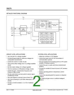
X9279
PRINCIPLES OF OPERATION
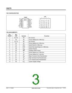
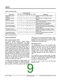
These switches are controlled by a Wiper Counter
Register (WCR). The 8-bits of the WCR (WCR[7:0])
are decoded to select, and enable, one of 256 switches
(see Table 1).
The X9279 is a integrated microcircuit incorporating a
resistor array and associated registers and counter
and the serial interface logic providing direct
communication between the host and the digitally
controlled potentiometers. This section provides detail
description of the following:
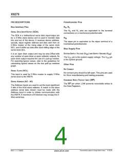
The WCR may be written directly. These Data
Registers can the WCR can be read and written by the
host system.
– Resistor Array Description.
Power Up and Down Recommendations.
There are no restrictions on the power-up or power-
– Serial Interface Description.
– Instruction and Register Description.
down conditions of V and the voltages applied to the
CC
potentiometer pins provided that V
is always more
CC
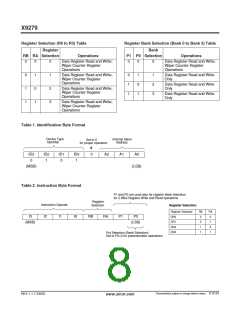
Array Description
positive than or equal to V , V , and V , i.e., V ≥ V ,
H L W CC H
V , V . The V ramp rate specification is always in
CC
The X9279 is comprised of a resistor array (see Figure
1). The array contains, in effect, 255 discrete resistive
segments that are connected in series. The physical
ends of each array are equivalent to the fixed terminals
L
W
effect.
of a mechanical potentiometer (R and R inputs).
H
L
At both ends of each array and between each resistor
segment is a CMOS switch connected to the wiper
(R ) output. Within each individual array only one
W
switch may be turned on at a time.
Figure 1. Detailed Potentiometer Block Diagram
SERIAL
BUS
SERIAL DATA PATH
R
H
FROM INTERFACE
CIRCUITRY
INPUT
C
O
U
N
T
REGISTER 0
(DR0)
REGISTER 1
(DR1)
8
8
PARALLEL
BUS
INPUT
E
R
BANK_0 Only
REGISTER 2
(DR2)
REGISTER 3
(DR3)
D
E
C
O
D
E
WIPER
COUNTER
REGISTER
(WCR)
INC/DEC
LOGIC
IF WCR = 00[H] THEN R = R
W
L
UP/DN
UP/DN
CLK
IF WCR = FF[H] THEN R = R
W
H
R
MODIFIED SCK
L
R
W
Characteristics subject to change without notice. 5 of 24
REV 1.1.7 2/6/03
www.xicor.com

 XICOR [ XICOR INC. ]