X4043/45
ABSOLUTE MAXIMUM RATINGS
COMMENT
Temperature under bias ................... -65°Cto+135°C
Storage temperature ........................ -65°C to +150°C
Voltage on any pin with
Stresses above those listed under “Absolute Maximum
Ratings” may cause permanent damage to the device.
This is a stress rating only; the functional operation of
the device (at these or any other conditions above those
listed in the operational sections of this specification) is
not implied. Exposure to absolute maximum rating con-
ditions for extended periods may affect device reliability.
respect to V .......................................-1.0V to +7V
SS
D.C. output current ............................................... 5mA
Lead temperature (soldering, 10 seconds)........ 300°C
RECOMMENDED OPERATING CONDITIONS
Temperature
Commercial
Industrial
Min.
0°C
Max.
70°C
Option
–2.7 and –2.7A
Blank and –4.5A
Supply Voltage Limits
2.7V to 5.5V
-40°C
+85°C
4.5V to 5.5V
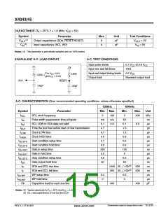
D.C. OPERATING CHARACTERISTICS (Over the recommended operating conditions unless otherwise specified.)
= 2.7 to 5.5V
V
CC
Symbol
Parameter
Min.
Max.
1.0
3.0
1
Unit
mA
mA
µA
Test Conditions
(1)
I
I
I
Active supply current read
Active supply current write
Standby current AC (WDT off)
V
= V x 0.1, V = V x 0.9
CC1
CC2
IL
CC
IH
CC
(1)
f
= 400kHz
SCL
(2)
V
= V x 0.1, V = V x 0.9
CC IH CC
SB1
IL
f
= 400kHz, SDA = open
SCL
V
= 1.22 x V min
CC
CC
(2)
(2)
I
I
Standby current DC (WDT off)
Standby current DC (WDT on)
1
µA
µA
V
= V
= V
SB2
SDA
SCL SB
Others = GND or V
SB
SB
20
V
=V
= V
SB3
SDA
SCL SB
Others = GND or V
I
Input leakage current
Output leakage current
10
10
µA
µA
V
V
= GND to V
CC
LI
IN
I
= GND to V
CC
LO
SDA
device is in standby
(3)
V
Input LOW voltage
Input nonvolatile
-0.5
V
V
x 0.3
V
V
IL
CC
(3)
V
V
V
x 0.7
+ 0.5
IH
CC
CC
Schmitt trigger input hysteresis
Fixed input level
HYS
0.2
.05 x V
V
V
V
related level
CC
CC
V
Output LOW voltage
0.4
V
I
I
= 3.0mA (2.7–5.5V)
= 1.8mA (2.0–3.6V)
OL
OL
OL
Notes: (1) The device enters the active state after any start, and remains active until: 9 clock cycles later if the device select bits in the slave
address byte are incorrect; 200ns after a stop ending a read operation; or t after a stop ending a write operation.
WC
(2) The device goes into standby: 200ns after any stop, except those that initiate a nonvolatile write cycle; t
after a stop that initiates
WC
a nonvolatile cycle; or 9 clock cycles after any start that is not followed by the correct device select bits in the slave address byte.
(3) V min. and V max. are for reference only and are not tested.
IL
IH
Characteristics subject to change without notice. 14 of 25
REV 1.1.17 9/14/01
www.xicor.com

 XICOR [ XICOR INC. ]