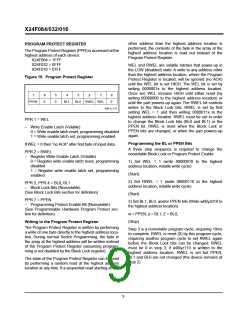
X24F064/032/016
DEVICE OPERATION
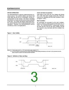
Clock and Data Conventions
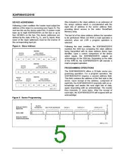
Data states on the SDA line can change only during
SCL LOW. SDA state changes during SCL HIGH are
reserved for indicating start and stop conditions. Refer
to Figures 1 and 2.
The X24F064/032/016 supports a bidirectional bus ori-
ented protocol. The protocol defines any device that
sends data onto the bus as a transmitter, and the re-
ceiving device as the receiver. The device controlling
the transfer is a master and the device being controlled
is the slave. The master will always initiate data trans-
fers, and provide the clock for both transmit and receive
operations. Therefore, the X24F064/032/016 will be
considered a slave in all applications.
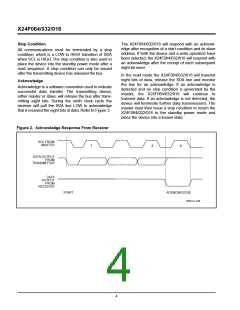
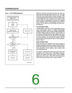
Start Condition
All commands are preceded by the start condition,
which is a HIGH to LOW transition of SDA when SCL is
HIGH. The X24F064/032/016 continuously monitors
the SDA and SCL lines for the start condition and will
not respond to any command until this condition has
been met.
Figure 1. Data Validity
SCL
SDA
DATA STABLE
DATA
CHANGE
6686 ILL F04
Notes: (5) Typical values are for T = 25°C and nominal supply voltage (2.7V)
A
(6) t is the minimum cycle time from the system perspective when polling techniques are not used. It is the maximum time the
PR
device requires to perform the internal program operation.
Figure 2. Definition of Start and Stop
SCL
SDA
START BIT
STOP BIT
6686 ILL F05
3

 XICOR [ XICOR INC. ]