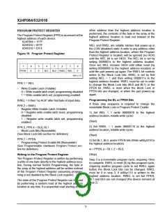
APPLICATION
NOTE
A V A I L A B L E
AN76 • AN78 • AN81 • AN87
64K/32K/16K
8K/4K/2K x 8 Bit
X24F064/032/016
SerialFlashTM Memory with Block LockTM Protection
FEATURES
DESCRIPTION
• 1.8V to 3.6V or 5V “Univolt” Read and
Program Power Supply Versions
• Low Power CMOS
The X24F064/032/016 is
a
CMOS SerialFlash
Memory Family, internally organized 8K/4K/2K x 8.
The family features a serial interface and software
protocol allowing operation on a simple two wire bus.
—Active Read Current Less Than 1mA
—Active Program Current Less Than 3mA
—Standby Current Less Than 1µA
• Internally Organized 8K/4K/2K x 8
• New Programmable Block Lock Protection
—Software Write Protection
—Programmable hardware Write Protect
• Block Lock (0, 1/4, 1/2, or all of the Flash
Memory array)
Device select inputs (S , S , S ) allow up to eight
0
1
2
devices to share a common two wire bus.
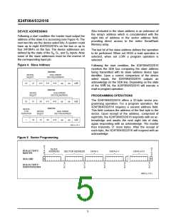
A Program Protect Register accessed at the highest
address location, provides three new programming
protection features: Software Programming Protection,
Block Lock Protection, and Hardware Programming
Protection. The Software Programming Protection
feature prevents any nonvolatile writes to the device
until the WEL bit in the program protect register is set.
The Block LockTM Protection feature allows the user to
individually protect four blocks of the array by program-
ming two bits in the programming protect register. The
Programmable Hardware Program Protect feature
allows the user to install each device with PP tied to
• 2 Wire Serial Interface
• Bidirectional Data Transfer Protocol
• 32 Byte Sector Programming
• Self Timed Program Cycle
—Typical Programming Time of 5ms
Per Sector
• High Reliability
—Endurance: 100,000 cycles per byte
—Data Retention: 100 Years
• Available Packages
V
, program the entire memory array in place, and
CC
then enable the hardware programming protection by
programming a PPEN bit in the program protect
register. After this, selected blocks of the array,
including the program protect register itself, are
permanently protected from being programmed.
—8-Lead PDIP
—8-Lead SOIC (JEDEC)
—14-Lead TSSOP (X24F032/016)
—20-Lead TSSOP (X24F064)
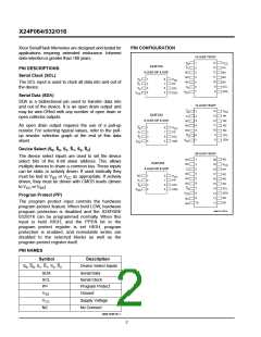
FUNCTIONAL DIAGRAM
DATA REGISTER
SDA
SECTOR DECODE LOGIC
SCL
32
8
X
DECODE
LOGIC
COMMAND
DECODE
AND CONTROL
LOGIC
SECTORED
MEMORY
ARRAY
S0/S0
S1/S1
S2/S2
PROGRAM
PROTECT
REGISTER
HIGH VOLTAGE
CONTROL
PROGRAMMING
CONTROL LOGIC
PP
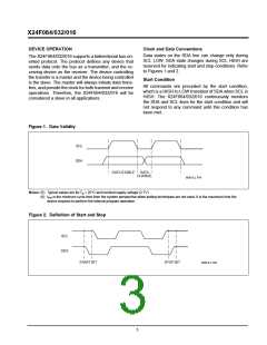
SerialFlash Memory and Block Lock
Protection are trademarks of Xicor, Inc.
6686 ILL F01.5
Xicor, 1995, 1996 Patents Pending
6686-3.8 8/29/96 T3/C0/D0 SH
Characteristics subject to change without notice
1

 XICOR [ XICOR INC. ]