X24F064/032/016
other address than the highest address location is
performed, the contents of the byte in the array at the
highest address location is read out instead of the
Program Protect Register.
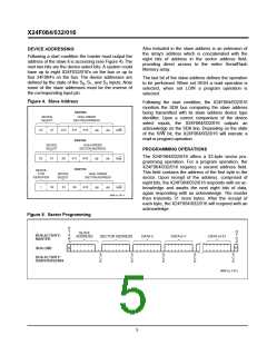
PROGRAM PROTECT REGISTER
The Program Protect Register (PPR) is accessed at the
highest address of each device:
X24F064 = 1FFF
X24F032 = 0FFF
X24F016 = 07FF
WEL and RWEL are volatile latches that power-up in
the LOW (disabled) state. A write to any address other
than the highest address location, where the Program
Protect Register is located, will be ignored (no ACK)
until the WEL bit is set HIGH. The WEL bit is set by
writing 0000001x to the highest address location.
Once set, WEL remains HIGH until either reset (by
writing 00000000 to the highest address location) or
until the part powers-up again. The RWEL bit controls
writes to the Block Lock bits. RWEL is set by first
setting WEL = 1 and then writing 0000011x to the
highest address location. RWEL must be set in order
to change the Block Lock bits (BL0 and BL1) or the
PPEN bit. RWEL is reset when the Block Lock or
PPEN bits are changed, or when the part powers-up
again.
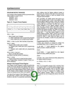
Figure 10. Program Protect Register
7
6
5
4
3
1
0
0
2
PPEN
0
0
BL1
BL0
WEL
RWEL
6686 ILL F15
PPR.1 = WEL
– Write Enable Latch (Volatile)
0 = Write enable latch reset, programming disabled
1 = Write enable latch set, programming enabled
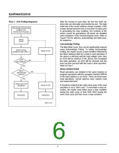
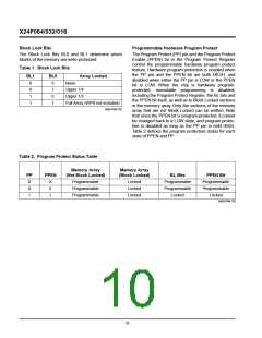
Programming the BL or PPEN Bits
If WEL = 0 then “no ACK” after first byte of input data.
A three step sequence is required to change the
nonvolatile Block Lock or Program Protect Enable:
PPR.2 = RWEL
– Register Write Enable Latch (Volatile)
0 = Register write enable latch reset, programming
disabled
1) Set WEL = 1 (write 00000010 to the highest
address location, volatile write cycle)
1 = Register write enable latch set, programming
enabled
(Start)
2) Set RWEL = 1 (write 00000110 to the highest
address location, volatile write cycle)
PPR.3, PPR.4 = BL0, BL1
– Block Lock Bits (Nonvolatile)
(See Block Lock Bits section for definition)
(Start)
PPR.7 = PPEN
3) Set BL1, BL0, and/or PPEN bits (Write w00yz010 to
the highest address location)
– Programming Protect Enable Bit (Nonvolatile)
(See Programmable Hardware Program Protect sec-
tion for definition)
w = PPEN, y = BL1, Z = BL0,
(Stop)
Writing to the Program Protect Register
The Program Protect Register is written by performing
a write of one byte directly to the highest address loca-
tion. During normal Sector Programming, the byte in
the array at the highest address will be written instead
of the Program Protect Register (assuming program-
ming is not disabled by the Block Lock register).
Step 3 is a nonvolatile program cycle, requiring 10ms
to complete. RWEL is reset (0) by this program cycle,
requiring another program cycle to set RWEL again
before the Block Lock bits can be changed. RWEL
must be 0 in step 3; if w00yz110 is written to the
highest address location, RWEL is set but PPEN,
BL1 and BL0 are not changed (the device remains at
step 2).
The state of the Program Protect Register can be read
by performing a random read at the highest address
location at any time. If a sequential read starting at any
9

 XICOR [ XICOR INC. ]