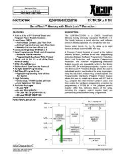
X24F064/032/016
Xicor SerialFlash Memories are designed and tested for
applications requiring extended endurance. Inherent
data retention is greater than 100 years.
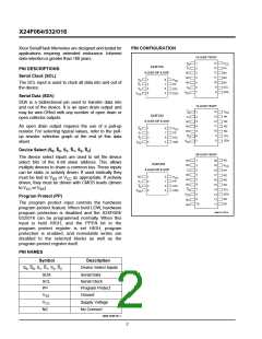
PIN CONFIGURATION
14-LEAD TSSOP
V
S
S
14
13
12
11
10
9
1
2
3
4
5
6
7
CC
0
X24F016
PP
PIN DESCRIPTIONS
Serial Clock (SCL)
1
8-LEAD DIP & SOIC
NC
NC
NC
NC
NC
S
S
S
1
2
3
4
8
7
6
5
V
0
1
2
CC
NC
The SCL input is used to clock all data into and out of
the device.
PP
SCL
SDA
S
2
SCL
SDA
8
V
V
SS
SS
Serial Data (SDA)
SDA is a bidirectional pin used to transfer data into
and out of the device. It is an open drain output and
may be wire-ORed with any number of open drain or
open collector outputs.
14-LEAD TSSOP
V
S
0
14
13
12
11
10
9
1
2
3
4
5
6
7
CC
X24F032
S
1
PP
8-LEAD DIP & SOIC
NC
NC
NC
NC
NC
An open drain output requires the use of a pull-up
resistor. For selecting typical values, refer to the pull-
up resistor selection graph at the end of this data
sheet.
S
0
S
1
S
2
1
2
3
4
8
7
6
5
V
CC
NC
PP
SCL
SDA
S
2
SCL
SDA
8
V
V
SS
SS
Device Select (S , S , S , S , S , S )
0
0
1
1
2
2
20-LEAD TSSOP
The device select inputs are used to set the device
select bits of the 8-bit slave address. This allows
multiple devices to share a common bus. These inputs
can be static or actively driven. If used statically they
NC
NC
NC
20
19
18
17
16
15
14
13
12
11
1
2
3
4
5
6
7
8
9
10
X24F064
V
CC
8-LEAD DIP & SOIC
S
1
PP
NC
NC
NC
NC
NC
NC
SCL
SDA
NC
NC
NC
1
2
3
4
8
7
6
5
V
must be tied to V or V
as appropriate. If actively
CC
SS
CC
S
1
PP
driven, they must be driven with CMOS levels (driven
to V or V ).
S
2
SCL
SDA
CC
SS
S
2
V
SS
V
SS
NC
NC
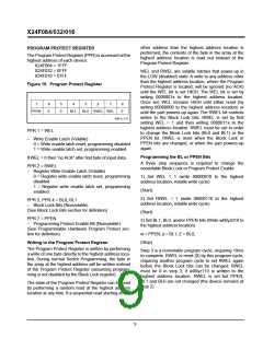
Program Protect (PP)
The program protect input controls the hardware
program protect feature. When held LOW, hardware
program protection is disabled and the X24F064/
032/016 can be programmed normally. When this
input is held HIGH, and the PPEN bit in the
program protect register is set HIGH, program
protection is enabled, and nonvolatile writes are
disabled to the selected blocks as well as the
program protect register itself.
6686 ILL F02.4
PIN NAMES
Symbol
Description
Device Select Inputs
S0, S0, S1, S1, S2, S2
SDA
SCL
PP
Serial Data
Serial Clock
Program Protect
Ground
VSS
VCC
NC
Supply Voltage
No Connect
6686 FRM T01.1
2

 XICOR [ XICOR INC. ]