WM8983
Product Preview
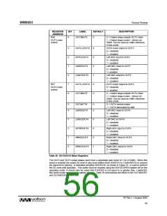
REGISTER
ADDRESS
BIT
LABEL
DEFAULT
DESCRIPTION
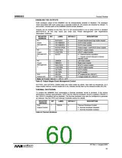
R56
6
OUT3MUTE
0
0 = Output stage outputs OUT3 mixer
OUT3 mixer
control
1 = Output stage muted – drives out
VMID. Can be used as VMID reference
in this mode.
3
2
1
0
7
6
OUT4_2OUT3
BYPL2OUT3
LMIX2OUT3
LDAC2OUT3
OUT3_2OUT4
OUT4MUTE
0
0
0
1
0
0
OUT4 mixer output to OUT3
0 = disabled
1 = enabled
Left ADC input to OUT3
0 = disabled
1 = enabled
Left DAC mixer to OUT3
0 = disabled
1= enabled
Left DAC output to OUT3
0 = disabled
1 = enabled
R57
OUT3 mixer output to OUT4
0 = disabled
OUT4 mixer
control
1= enabled
0 = Output stage outputs OUT4 mixer
1 = Output stage muted – drives out
VMID. Can be used as VMID reference
in this mode.
5
4
OUT4ATTN
LMIX2OUT4
0
0
0 = OUT4 normal output
1 = OUT4 attenuated by 6dB
Left DAC mixer to OUT4
0 = disabled
1 = enabled
3
2
1
0
LDAC2OUT4
BYPR2OUT4
RMIX2OUT4
RDAC2OUT4
0
0
0
1
Left DAC to OUT4
0 = disabled
1 = enabled
Right ADC input to OUT4
0 = disabled
1 = enabled
Right DAC mixer to OUT4
0 = disabled
1 = enabled
Right DAC output to OUT4
0 = disabled
1 = enabled
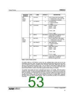
Table 38 OUT3/OUT4 Mixer Registers
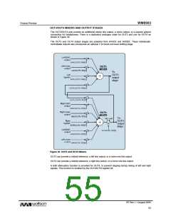
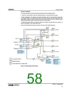
The OUT3 and OUT4 output stages each have a selectable gain boost of 1.5x (3.52dB). When this
boost is enabled the output DC level is also level shifted (from AVDD1/2 to 1.5xAVDD1/2) to prevent
the signal from clipping. A dedicated amplifier BUFDCOP, as shown in Figure 31, is used to perform
the DC level shift operation. This buffer must be enabled using the BUFDCOPEN register bit for this
operating mode. It should also be noted that if AVDD2 is not equal to or greater than 1.5xAVDD1
this boost mode may result in signals clipping. Table 35 summarises the effect of the OUT3BOOST
and OUT4BOOST control bits.
PP Rev 1.1 August 2005
56
w

 WOLFSON [ WOLFSON MICROELECTRONICS PLC ]