WM8983
Product Preview
REGISTER
ADDRESS
BIT
LABEL
DEFAULT
DESCRIPTION
R49
2
SPKBOOST
0
0 = speaker gain = -1;
DC = AVDD1 / 2
Output control
1 = speaker gain = +1.5;
DC = 1.5 x AVDD1 / 2
R1
8
BUFDCOPEN
0
Dedicated buffer for DC level shifting
output stages when in 1.5x gain
boost configuration.
Power
management
1
0 = Buffer disabled
1 = Buffer enabled (required for 1.5x
gain boost)
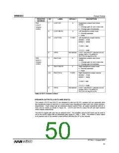
Table 34 Speaker Boost Stage Control
SPKBOOST
OUTPUT
STAGE GAIN
OUTPUT DC
LEVEL
OUTPUT STAGE
CONFIGURATION
0
1
1x (0dB)
AVDD1/2
Inverting
1.5x (3.52dB)
1.5xAVDD1/2
Non-inverting
Table 35 Output Boost Stage Details
REGISTER
ADDRESS
BIT
LABEL
DEFAULT
DESCRIPTION
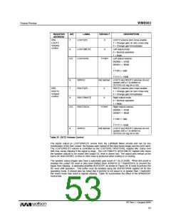
R43
Beep control
5
MUTERPGA2INV
INVROUT2
0
0
Mute input to INVROUT2 mixer
Invert ROUT2 output
AUXR input to ROUT2 inverter gain
000 = -15dB
4
3:1
BEEPVOL
000
001 = -12dB
010 = -9dB
011 = -6dB
100 = -3dB
101 = 0dB
110 = +3dB
111 = +6dB
0
BEEPEN
0
0 = mute AUXR beep input
1 = enable AUXR beep input
Table 36 AUXR – ROUT2 BEEP Mixer Function
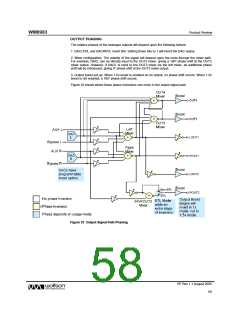
ZERO CROSS TIMEOUT
A zero-cross timeout function is provided so that if zero cross is enabled on the input or output PGAs
the gain will automatically update after a timeout period if a zero cross has not occurred. This is
enabled by setting SLOWCLKEN. The timeout period is dependent on the clock input to the digital
and is equal to 221 * SYSCLK period.
REGISTER
ADDRESS
BIT
LABEL
DEFAULT
DESCRIPTION
R7
0
SLOWCLKEN
0
Slow clock enable. Used for both the
jack insert detect debounce circuit and
the zero cross timeout.
Additional
Control
0 = slow clock disabled
1 = slow clock enabled
Table 37 Timeout Clock Enable Control
PP Rev 1.1 August 2005
54
w

 WOLFSON [ WOLFSON MICROELECTRONICS PLC ]