Product Preview
WM8983
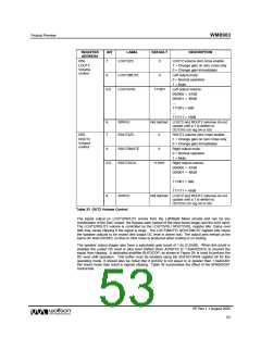
REGISTER
ADDRESS
BIT
LABEL
LOUT2ZC
DEFAULT
DESCRIPTION
R54
7
0
LOUT2 volume zero cross enable:
1 = Change gain on zero cross only
0 = Change gain immediately
Left output mute:
0 = Normal operation
1 = Mute
LOUT2
Volume
control
6
LOUT2MUTE
LOUT2VOL
0
5:0
111001
Left output volume:
000000 = -57dB
000001 = -56dB
...
111001 = 0dB
...
111111 = +6dB
8
7
SPKVU
Not latched LOUT2 and ROUT2 volumes do not
update until a 1 is written to
OUT2VU (in reg 54 or 55)
R55
ROUT2ZC
0
ROUT2 volume zero cross enable:
1 = Change gain on zero cross only
0 = Change gain immediately
Right output mute:
0 = Normal operation
1 = Mute
ROUT2
Volume
control
6
ROUT2MUTE
ROUT2VOL
0
5:0
111001
Right output volume:
000000 = -57dB
000001 = -56dB
...
111001 = 0dB
...
111111 = +6dB
8
SPKVU
Not latched LOUT2 and ROUT2 volumes do not
update until a 1 is written to
OUT2VU (in reg 54 or 55)
Table 33 OUT2 Volume Control
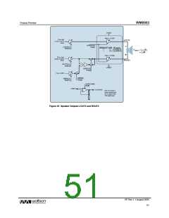
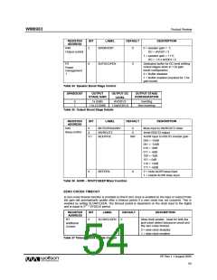
The signal output on LOUT2/ROUT2 comes from the Left/Right Mixer circuits and can be any
combination of the DAC output, the Bypass path (output of the input boost stage) and the AUX input.
The LOUT2/ROUT2 volume is controlled by the LOUT2VOL/ ROUT2VOL register bits. Gains over
0dB may cause clipping if the signal is large. The LOUT2MUTE/ ROUT2MUTE register bits cause
the speaker outputs to be muted (the output DC level is driven out). The output pins remain at the
same DC level (DCOP), so that no click noise is produced when muting or un-muting
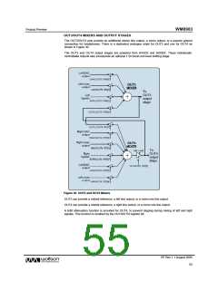
The speaker output stages also have a selectable gain boost of 1.5x (3.52dB). When this boost is
enabled the output DC level is also level shifted (from AVDD1/2 to 1.5xAVDD1/2) to prevent the
signal from clipping. A dedicated amplifier BUFDCOP, as shown in Figure 29, is used to perform the
DC level shift operation. This buffer must be enabled using the BUFDCOPEN register bit for this
operating mode. It should also be noted that if AVDD2 is not equal to or greater than 1.5xAVDD1
this boost mode may result in signals clipping. Table 35 summarises the effect of the SPKBOOST
control bits.
PP Rev 1.1 August 2005
53
w

 WOLFSON [ WOLFSON MICROELECTRONICS PLC ]