Product Preview
WM8983
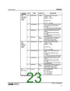
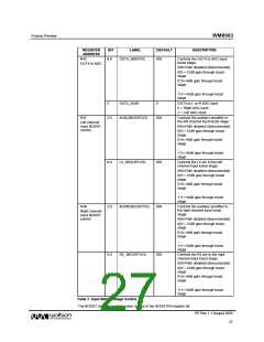
REGISTER
ADDRESS
BIT
LABEL
DEFAULT
DESCRIPTION
R42
OUT4 to ADC
8:6
OUT4_2ADCVOL
000
Controls the OUT4 to ADC input
boost stage:
000=Path disabled (disconnected)
001=-12dB gain through boost
stage
010=-9dB gain through boost
stage
…
111=+6dB gain through boost
stage
5
OUT4_2LNR
0
OUT4 to L or R ADC ni put
0 = Right ADC input
1 = Left ADC input
R47
2:0
AUXL2BOOSTVOL
000
Controls the auxiliary amplifier to
the left channel input boost stage:
Left channel
Input BOOST
control
000=Path disabled (disconnected)
001=-12dB gain through boost
stage
010=-9dB gain through boost
stage
…
111=+6dB gain through boost
stage
6:4
L2_2BOOSTVOL
000
Controls the L2 pin to the left
channel input boost stage:
000=Path disabled (disconnected)
001=-12dB gain through boost
stage
010=-9dB gain through boost
stage
…
111=+6dB gain through boost
stage
R48
2:0
AUXR2BOOSTVOL
000
Controls the auxiliary amplifier to
the right channel input boost
stage:
Right channel
Input BOOST
control
000=Path disabled (disconnected)
001=-12dB gain through boost
stage
010=-9dB gain through boost
stage
…
111=+6dB gain through boost
stage
6:4
R2_2BOOSTVOL
000
Controls the R2 pin to the right
channel input boost stage:
000=Path disabled (disconnected)
001=-12dB gain through boost
stage
010=-9dB gain through boost
stage
…
111=+6dB gain through boost
stage
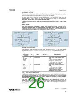
Table 7 Input BOOST Stage Control
The BOOST stage is enabled under control of the BOOSTEN register bit.
PP Rev 1.1 August 2005
27
w

 WOLFSON [ WOLFSON MICROELECTRONICS PLC ]