WM8983
Product Preview
DESCRIPTION
REGISTER
ADDRESS
BIT
LABEL
DEFAULT
R2
4
BOOSTENL
0
0
Left channel Input BOOST enable
0 = Boost stage OFF
Power
management
2
1 = Boost stage ON
5
BOOSTENR
Right channel Input BOOST enable
0 = Boost stage OFF
1 = Boost stage ON
Table 8 Input BOOST Enable Control
MICROPHONE BIASING CIRCUIT
The MICBIAS output provides a low noise reference voltage suitable for biasing electret type
microphones and the associated external resistor biasing network. Refer to the Applications
Information section for recommended external components. The MICBIAS voltage can be altered via
the MBVSEL register bit. When MBVSEL=0, MICBIAS=0.9*AVDD1 and when MBVSEL=1,
MICBIAS=0.65*AVDD1. The output can be enabled or disabled using the MICBEN control bit.
REGISTER
ADDRESS
BIT
LABEL
DEFAULT
DESCRIPTION
R1
4
MICBEN
0
Microphone Bias Enable
Power
management 1
0 = OFF (high impedance output)
1 = ON
Table 9 Microphone Bias Enable Control
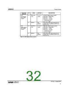
REGISTER
ADDRESS
BIT
LABEL
DEFAULT
DESCRIPTION
R44
Input control
8
MBVSEL
0
Microphone Bias Voltage Control
0 = 0.9 * AVDD1
1 = 0.65 * AVDD1
Table 10 Microphone Bias Voltage Control
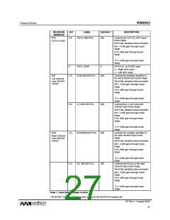
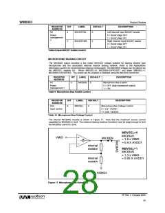
The internal MICBIAS circuitry is shown in Figure 17. Note that the maximum source current
capability for MICBIAS is 3mA. The external biasing resistors therefore must be large enough to limit
the MICBIAS current to 3mA.
MBVSEL=0
MICBIAS
= 1.8 x VMID
VMID
MICBEN
= 0.9 X AVDD1
internal
resistor
MBVSEL=1
MICBIAS
= 1.3 x VMID
= 0.65 X AVDD1
internal
resistor
AGND1
Figure 17 Microphone Bias Schematic
PP Rev 1.1 August 2005
28
w

 WOLFSON [ WOLFSON MICROELECTRONICS PLC ]