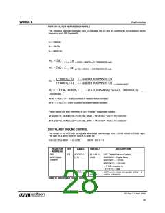
WM8976
Pre-Production
REGISTER
ADDRESS
BIT
LABEL
DEFAULT
DESCRIPTION
R47
2:0
AUXL2BOOSTVOL
000
Controls the auxilliary amplifer to
the input boost stage:
Input BOOST
control
000=Path disabled (disconnected)
001=-12dB gain through boost
stage
010=-9dB gain through boost
stage
…
111=+6dB gain through boost
stage
6:4
L2_2BOOSTVOL
000
Controls the L2 pin to the input
boost stage:
000=Path disabled (disconnected)
001=-12dB gain through boost
stage
010=-9dB gain through boost
stage
…
111=+6dB gain through boost
stage
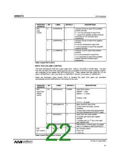
Table 7 Input BOOST Stage Control
The BOOST stage is enabled under control of the BOOSTEN register bit.
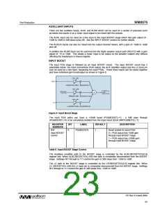
REGISTER
ADDRESS
BIT
LABEL
DEFAULT
DESCRIPTION
R2
4
BOOSTENL
0
Input BOOST enable
Power
management
2
0 = Boost stage OFF
1 = Boost stage ON
Table 8 Input BOOST Enable Control
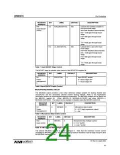
MICROPHONE BIASING CIRCUIT
The MICBIAS output provides a low noise reference voltage suitable for biasing electret type
microphones and the associated external resistor biasing network. Refer to the Applications
Information section for recommended external components. The MICBIAS voltage can be altered via
the MBVSEL register bit.
When MBVSEL=0, MICBIAS=0.9*AVDD and when MBVSEL=1,
MICBIAS=0.65*AVDD. The output can be enabled or disabled using the MICBEN control bit.
REGISTER
ADDRESS
BIT
LABEL
DEFAULT
DESCRIPTION
Microphone Bias Enable
R1
4
MICBEN
0
Power
management 1
0 = OFF (high impedance output)
1 = ON
Table 9 Microphone Bias Enable Control
REGISTER
ADDRESS
BIT
LABEL
DEFAULT
DESCRIPTION
R44
Input control
8
MBVSEL
0
Microphone Bias Voltage Control
0 = 0.9 * AVDD
1 = 0.65 * AVDD
Table 10 Microphone Bias Voltage Control
The internal MICBIAS circuitry is shown in Figure 9. Note that the maximum source current
capability for MICBIAS is 3mA. The external biasing resistors therefore must be large enough to limit
the MICBIAS current to 3mA.
PP Rev 3.0 April 2006
24
w

 WOLFSON [ WOLFSON MICROELECTRONICS PLC ]