WM8959
Pre-Production
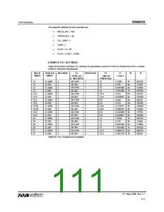
3-WIRE / 4-WIRE SERIAL CONTROL MODES
The WM8959 is controlled by writing to registers through a 3- or 4-wire serial control interface. A
control word consists of 24 bits. The first bit is the read/write bit (R/W), which is followed by 7
address bits (A6 to A0) that determine which control register is accessed. The remaining 16 bits (B15
to B0) are data bits, corresponding to the 16 bits in each control register.
The 3- or 4-wire modes are selected by the RD_3W_ENA register bit. Additionally the MODE_3W4W
control bit can be used to select between push 0/1 and open-drain or wired-OR modes, as described
in Table 69 below.
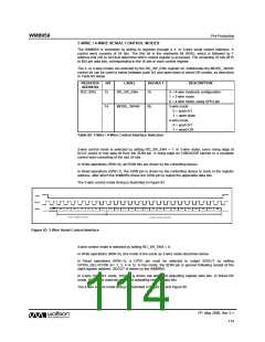
REGISTER
ADDRESS
BIT
15
LABEL
DEFAULT
DESCRIPTION
R22 (16h)
RD_3W_ENA
1b
3- / 4-wire readback configuration
1 = 3-wire mode
0 = 4-wire mode, using GPIO pin
3-wire mode
14
MODE_3W4W
0b
0 = push 0/1
1 = open-drain
4-wire mode
0 = push 0/1
1 = wired-OR
Table 69 3-Wire / 4-Wire Control Interface Selection
3-wire control mode is selected by setting RD_3W_ENA = 1. In 3-wire mode, every rising edge of
SCLK clocks in one data bit from the SDIN pin. A rising edge on CSB/ADDR latches in a complete
control word consisting of the last 24 bits.
In Write operations (R/W=0), all SDIN bits are driven by the controlling device.
In Read operations (R/W=1), the SDIN pin is driven by the controlling device to clock in the register
address, after which the WM8959 drives the SDIN pin to output the applicable data bits.
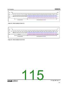
The 3-wire control mode timing is illustrated in Figure 83.
Figure 83 3-Wire Serial Control Interface
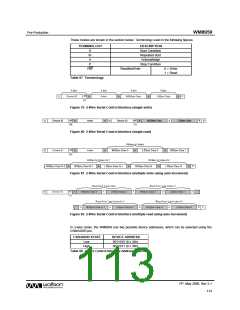
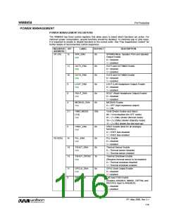
4-wire control mode is selected by setting RD_3W_ENA = 0.
In Write operations (R/W=0), this mode is the same as 3-wire mode described above.
In Read operations (R/W=1), a GPIO pin must be selected to output SDOUT by setting
GPIOn_SEL=0110b (n= 1, 3, 4 or 5). In this mode, the SDIN pin is ignored following receipt of the
valid register address. SDOUT is driven by the WM8959.
In 4-wire Push 0/1 mode, SDOUT is driven low when not outputting register data bits. In Wired-OR
mode, SDOUT is undriven when not outputting register data bits.
The 4-wire control mode timing is illustrated in Figure 84 and Figure 85.
PP, May 2008, Rev 3.1
114
w

 WOLFSON [ WOLFSON MICROELECTRONICS PLC ]