WM8959
Pre-Production
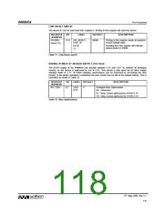
CHIP RESET AND ID
The device ID can be read back from register 0. Writing to this register will reset the device.
REGISTER
ADDRESS
BIT
LABEL
DEFAULT
DESCRIPTION
R0 (00h)
15:0
SW_RESET_
CHIP_ID
8990h
Writing to this register resets all registers
to their default state.
Reset / ID
[15:0]
(rr)
Reading from this register will indicate
device family ID 8990h.
Table 71 Chip Reset and ID
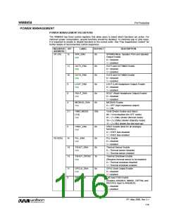
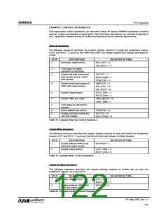
SAVING POWER AT HIGHER SUPPLY VOLTAGE
The AVDD supply of the WM8959 can operate between 2.7V and 3.6V. By default, all analogue
circuitry on the device is optimized to run at 3.3V. This set-up is also good for all other supply
voltages down to 2.7V. At lower voltages, performance can be improved by increasing the bias
current. If low power operation is preferred the bias current can be left at the default setting. This is
controlled as shown in Table 72.
REGISTER
ADDRESS
BIT
LABEL DEFAULT
DESCRIPTION
R51 (33h)
8:7
VSEL
[1:0]
11
Analogue Bias Optimisation
00 = Reserved
01 = Bias current optimized for AVDD=2.7V
1X = Bias current optimized for AVDD=3.3V
Table 72 Bias Optimisation
PP, May 2008, Rev 3.1
118
w

 WOLFSON [ WOLFSON MICROELECTRONICS PLC ]