Production Data
WM8912
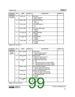
REGISTER
ADDRESS
BIT
LABEL
DEFAULT
DESCRIPTION
REFER TO
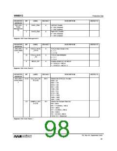
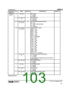
R22 (16h)
Clock Rates
2
15
MCLK_INV
0
MCLK Invert
0 = MCLK not inverted
1 = MCLK inverted
SYSCLK Source Select
0 = MCLK
14
12
3
SYSCLK_SRC
TOCLK_RATE
OPCLK_ENA
0
0
0
0
0
0
1 = FLL output
TOCLK Rate Divider (/2)
0 = f / 2
1 = f / 1
GPIO Clock Output Enable
0 = disabled
1 = enabled
2
CLK_SYS_EN
A
System Clock enable
0 = Disabled
1 = Enabled
1
CLK_DSP_EN
A
DSP Clock enable
0 = Disabled
1 = Enabled
0
TOCLK_ENA
Zero Cross timeout enable
0 = Disabled
1 = Enabled
Register 16h Clock Rates 2
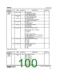
REGISTER
ADDRESS
BIT
LABEL
DEFAULT
DESCRIPTION
REFER TO
R24 (18h)
Audio
Interface 0
12
DACL_DATINV
0
Left DAC Invert
0 = Left DAC output not inverted
1 = Left DAC output inverted
Right DAC Invert
11
DACR_DATIN
V
0
0 = Right DAC output not inverted
1 = Right DAC output inverted
DAC Digital Input Volume Boost
00 = 0dB
10:9
DAC_BOOST
[1:0]
00
01 = +6dB (Input data must not exceed -6dBFS)
10 = +12dB (Input data must not exceed -12dBFS)
11 = +18dB (Input data must not exceed -18dBFS)
Left DAC Data Source Select
0 = Left DAC outputs left channel data
1 = Left DAC outputs right channel data
Right DAC Data Source Select
0 = Right DAC outputs left channel data
1 = Right DAC outputs right channel data
DAC Companding Enable
5
4
1
0
AIFDACL_SRC
0
1
0
0
AIFDACR_SR
C
DAC_COMP
0 = disabled
1 = enabled
DAC_COMPM
ODE
DAC Companding Type
0 = μ-law
1 = A-law
Register 18h Audio Interface 0
PD, Rev 4.0, September 2010
99
w

 WOLFSON [ WOLFSON MICROELECTRONICS PLC ]