Production Data
WM8912
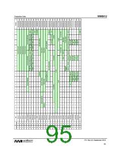
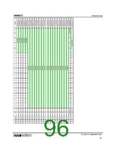
REGISTER BITS BY ADDRESS
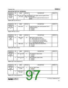
REGISTER
ADDRESS
BIT
LABEL
DEFAULT
DESCRIPTION
REFER TO
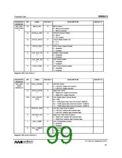
R0 (00h)
SW Reset
and ID
15:0
SW_RST_DEV 1000_1001 Writing to this register resets all registers to their
_ID1 [15:0] _0000_010 default state.
0
Reading from this register will indicate Device ID
8904h.
Register 00h SW Reset and ID
REGISTER
ADDRESS
BIT
LABEL
DEFAULT
DESCRIPTION
REFER TO
R4 (04h)
Bias Control
0
0
BIAS_ENA
0
Enables the Normal bias current generator (for all
analogue functions)
0 = Disabled
1 = Enabled
Register 04h Bias Control 0
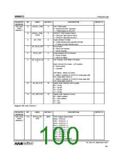
REGISTER
ADDRESS
BIT
LABEL
DEFAULT
DESCRIPTION
REFER TO
R5 (05h)
VMID
Control 0
2:1
VMID_RES
[1:0]
00
VMID Divider Enable and Select
00 = VMID disabled (for OFF mode)
01 = 2 x 50k divider (for normal operation)
10 = 2 x 250k divider (for low power standby)
11 = 2 x 5k divider (for fast start-up)
Enable VMID master bias current source
0 = Disabled
0
VMID_ENA
0
1 = Enabled
Register 05h VMID Control 0
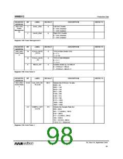
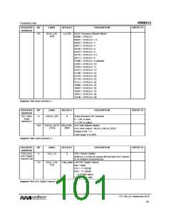
REGISTER
ADDRESS
BIT
LABEL
DEFAULT
DESCRIPTION
REFER TO
R14 (0Eh)
Power
Managemen
t 2
1
HPL_PGA_EN
A
0
Left Headphone Output Enable
0 = disabled
1 = enabled
0
HPR_PGA_EN
A
0
Right Headphone Output Enable
0 = disabled
1 = enabled
Register 0Eh Power Management 2
REGISTER
ADDRESS
BIT
LABEL
DEFAULT
DESCRIPTION
REFER TO
R15 (0Fh)
Power
Managemen
t 3
1
LINEOUTL_PG
A_ENA
0
Left Line Output Enable
0 = disabled
1 = enabled
0
LINEOUTR_P
GA_ENA
0
Right Line Output Enable
0 = disabled
1 = enabled
Register 0Fh Power Management 3
PD, Rev 4.0, September 2010
97
w

 WOLFSON [ WOLFSON MICROELECTRONICS PLC ]