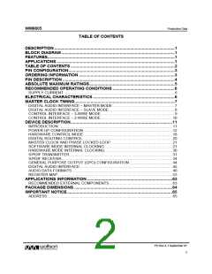
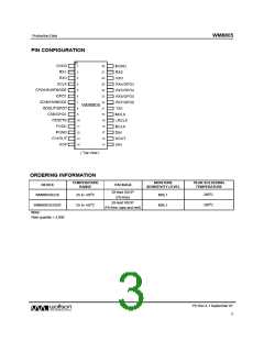
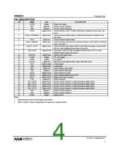
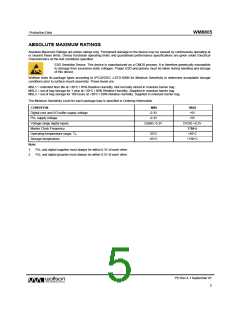
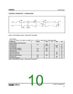
WM8805
Production Data
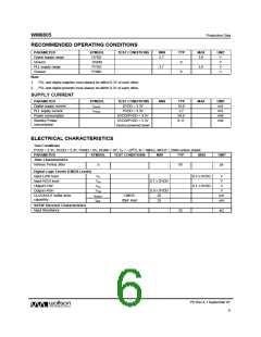
RECOMMENDED OPERATING CONDITIONS
PARAMETER
Digital supply range
Ground
SYMBOL
DVDD
TEST CONDITIONS
MIN
TYP
0
MAX
UNIT
2.7
3.6
V
V
V
V
DGND
PVDD
PLL supply range
Ground
2.7
3.6
PGND
0
Note:
1. PLL and digital supplies must always be within 0.3V of each other.
2. PLL and digital grounds must always be within 0.3V of each other.
SUPPLY CURRENT
PARAMETER
SYMBOL
IDVDD
TEST CONDITIONS
DVDD = 3.3V
MIN
TYP
14.9
1.7
MAX
UNIT
mA
Digital supply current
PLL supply current
Power consumption
IPVDD
PVDD = 3.3V
mA
DVDD/PVDD = 3.3V
DVDD/PVDD = 3.3V
Device powered down
54.8
0.11
mW
mW
Standby Power
consumption
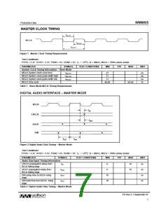
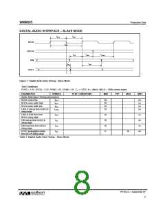
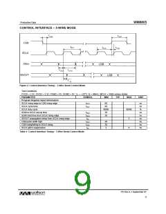
ELECTRICAL CHARACTERISTICS
Test Conditions
PVDD = 3.3V, DVDD = 3.3V, PGND = 0V, DGND = 0V, TA = +25oC, fs = 48kHz, MCLK = 256fs unless stated.
PARAMETER
SYMBOL
TEST CONDITIONS
MIN
TYP
MAX
UNIT
Jitter Characteristics
Intrinsic Period Jitter
Ji
50
ps
Digital Logic Levels (CMOS Levels)
Input LOW level
VIL
VIH
0.3 x DVDD
0.1 x DVDD
V
V
Input HIGH level
0.7 x DVDD
Output LOW
VOL
VOH
Isource
Isink
V
Output HIGH
0.9 x DVDD
V
CLOCKOUT buffer drive
capability
CMOS
25
25
mA
mA
20pF load
S/PDIF Receiver Characteristics
Input Resistance
23
kΩ
PD Rev 4.1 September 07
6
w

 WOLFSON [ WOLFSON MICROELECTRONICS PLC ]