Production Data
WM8805
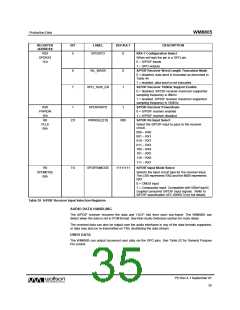
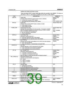
REGISTER
ADDRESS
BIT
LABEL
DEFAULT
DESCRIPTION
RX4-7 Configuration Select
R29
SPDRX1
1Ch
5
SPDGPO
0
When set high the pin is a GPO pin.
0 – S/PDIF inputs
1 – GPO outputs
6
7
WL_MASK
0
1
S/PDIF Receiver Word Length Truncation Mask
0 = disabled, data word is truncated as described in
Table 44.
1 = enabled, data word is not truncated.
SPD_192K_EN
S/PDIF Receiver 192kHz Support Enable
0 = disabled, S/PDIF receiver maximum supported
sampling frequency is 96kHz
1 = enabled, S/PDIF receiver maximum supported
sampling frequency is 192kHz
R30
PWRDN
1Eh
1
SPDIFRXPD
RXINSEL[2:0]
1
S/PDIF Receiver Powerdown
0 = S/PDIF receiver enabled
1 = S/PDIF receiver disabled
S/PDIF Rx Input Select
R8
2:0
000
PLL6
08h
Select the S/PDIF input to pass to the receiver
circuit.
000 – RX0
001 – RX1
010 – RX2
011 – RX3
100 – RX4
101 – RX5
110 – RX6
111 – RX7
R9
SPDMODE
09h
7:0
SPDIFINMODE
11111111
S/PDIF Input Mode Select
Selects the input circuit type for the receiver input.
The LSB represents RX0 and the MSB represents
RX7
0 = CMOS input
1 = Comparator input. Compatible with 500mVppAC
coupled consumer S/PDIF input signals. Refer to
S/PDIF specification (IEC 60958-3) for full details.
Table 39 S/PDIF Receiver Input Selection Registers
AUDIO DATA HANDLING
The S/PDIF receiver recovers the data and VUCP bits from each sub-frame. The WM8805 can
detect when the data is not in PCM format. See Non-Audio Detection section for more detail.
The received data can also be output over the audio interfaces in any of the data formats supported,
or data may also be re-transmitted on TX0, de-jittering the data stream.
USER DATA
The WM8805 can output recovered user data via the GPO pins. See Table 52 for General Purpose
Pin control.
PD Rev 4.1 September 07
35
w

 WOLFSON [ WOLFSON MICROELECTRONICS PLC ]