Production Data
WM8805
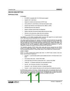
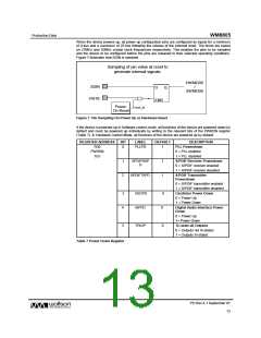
When the device powers up, all power up configuration pins are configured as inputs for a minimum
of 9.4us and a maximum of 25.6us following the release of the external reset. The times are based
on 27MHz and 10MHz crystal clock frequencies respectively. This enables the pins to be sampled
and the device to be configured before the pins are released to their selected operating conditions.
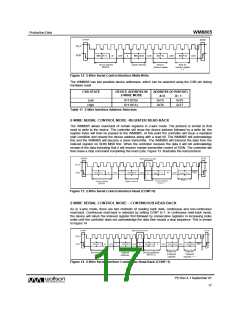
Figure 7 illustrates how SDIN is sampled.
Sampling of pin value at reset to
generate internal signals.
HWMODE
SDIN
/
D
Q
SWMODE
RSTB
ENB
Power-
POR_B
On Reset
Figure 7 Pin Sampling On Power Up or Hardware Reset
If the device is powered up in Software control mode, all functions of the device are powered down by
default and must be powered up individually by writing to the relevant bits of the PWRDN register
(Table 7). In Hardware Control Mode, all functions of the device are powered up by default.
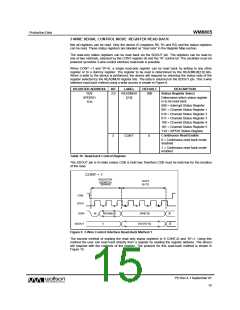
REGISTER ADDRESS
BIT
LABEL
DEFAULT
DESCRIPTION
PLL Powerdown
R30
PWRDN
1Eh
0
PLLPD
1
0 = PLL enabled
1 = PLL disabled
1
2
SPDIFRXP
D
1
1
S/PDIF Receiver Powerdown
0 = S/PDIF receiver enabled
1 = S/PDIF receiver disabled
SPDIFTXPD
S/PDIF Transmitter
Powerdown
0 = S/PDIF transmitter enabled
1 = S/PDIF transmitter disabled
Oscillator Power Down
0 = Power Up
3
4
OSCPD
AIFPD
0
0
1 = Power Down
Digital Audio Interface Power
Down
0 = Power Up
1= Power Down
5
TRIOP
0
Tri-state all Outputs
0 = Outputs not tri-stated
1 = Outputs tri-stated
Table 7 Power Down Register
PD Rev 4.1 September 07
13
w

 WOLFSON [ WOLFSON MICROELECTRONICS PLC ]