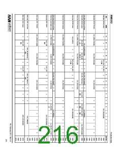
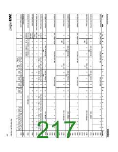
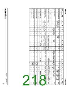
WM8352
Production Data
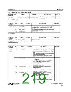
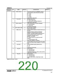
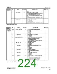
REFER TO
REGISTER
ADDRESS
BIT
LABEL
DEFAULT
DESCRIPTION
11:10
RSTB_TO[1:0]
11
Time that the /RST pin and /MEMRST output is
held low after the chip reaches the active state.
00 = 15ms
01 = 30ms
10 = 60ms
11 = 120ms
Default held in metal mask.
Bandgap sleep mode
0 = never in sleep mode
1 = sleep mode is controlled by Main SM
Default held in metal mask.
Halts watchdog timer for system debugging
0 = normal operation
1 = WDOG halt
9
7
BG_SLEEP
0
0
WDOG_DEBUG
Protected by security key.
[No description available]
Reset by state machine.
6
5
CHIP_RESET_ENA
MEM_VALID
0
0
Indicates that the contents of external memory are
still valid.
This bit is cleared on startup and whenever
/MEMRST is asserted from the main state
machine. The system software should set this bit
once the external memory has been set up.
Controlled in hibernate mode by
MEMRST_HIB_MODE
0 = External memory is not valid and needs
restoring.
1 = External memory is valid.
Reset when /MEMRST is asserted.
4
3
CHIP_SET_UP
ON_DEB_T
0
0
A spare register bit that can be used by the system
to say if the chip has been configured. It is reset by
POR.
ON pin Shutdown function debounce time
0 = 10s
1 = 5s
Protected by security key.
ON pin polarity:
1
0
ON_POL
IRQ_POL
1
0
0 = Active high (ON)
1 = Active low (/ON)
Protected by security key. Reset by state machine.
Default held in metal mask.
IRQ pin polarity:
0 = Active low (/IRQ)
1 = Active high (IRQ)
Reset by state machine. Default held in metal
mask.
Register 03h System Control 1
PD, February 2011, Rev 4.4
220
w

 WOLFSON [ WOLFSON MICROELECTRONICS PLC ]