Production Data
WM8352
27 REGISTER BITS BY ADDRESS
REGISTER BIT
ADDRESS
LABEL
DEFAULT
DESCRIPTION
REFER TO
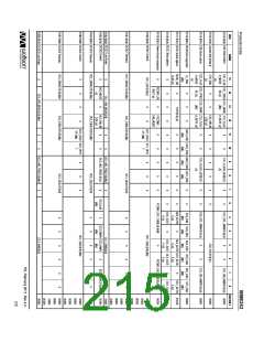
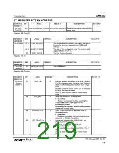
R0 (00h)
Reset/ID
15:0 SW_RESET/CHIP_ID[15:0] 0110_0001_0100_0011 Reading this register returns 6143h.
Never reset.
Register 00h Reset/ID
REGISTER
ADDRESS
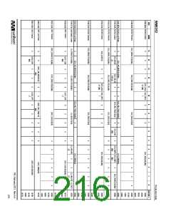
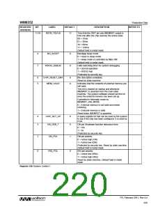
R1 (01h) ID
BIT
LABEL
DEFAULT
DESCRIPTION
REFER TO
15:12 CHIP_REV[3:0]
11:10 CONF_STS[1:0]
The functional silicon revision - this tracks changes in
functionality which are separate from ROM mask
settings
The state of the configuration pins. This selects what
register defaults should be.
7:0
CUST_ID[7:0]
The Chip Revision Number
Register 01h ID
REGISTER
ADDRESS
BIT
LABEL
DEFAULT
DESCRIPTION
REFER TO
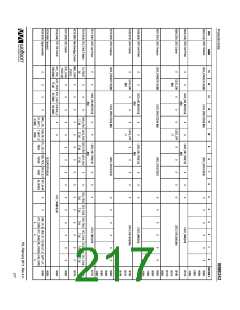
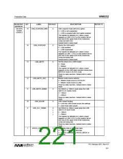
R2 (02h)
Revision
7:0
MASK_REV[7:0]
The ROM Mask ID
Register 02h Revision
REGISTER
ADDRESS
BIT
LABEL
DEFAULT
0
DESCRIPTION
REFER TO
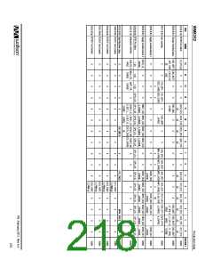
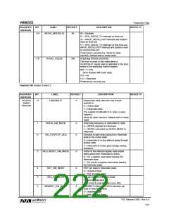
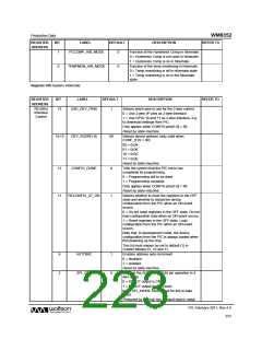
R3 (03h)
System
Control 1
15
CHIP_ON
Indicates whether the system is on or off. Writing
0 to this bit powers down the whole chip. Registers
which are affected by state machine reset will get
reset.
Once the system is turned OFF it can be restarted
by any of the valid ON event.
Reset by state machine. Default held in metal
mask.
14
SYS_RST
0
Allows the processors to reboot itself
0 = Do nothing
1 = Perform a processor reset by asserting the
/RST and /MEMRST (GPIO) pins for the
programmed duration
Protected by security key. Reset by state machine.
Default held in metal mask.
13
12
POWERCYCLE
VCC_FAULT_OV
0
1
Action to take on a fault (if response is set to
shutdown system):
0 = Shut down
1 = Shutdown everything then go through startup
sequence. i.e. Reboot the system.
Include over voltage in the /VCC_FAULT pin
(Alternative GPIO function)
0 = Do not include over voltage in the
/VCC_FAULT signal
1 = Include the over voltage in the /VCC_FAULT
signal
Reset by state machine. Default held in metal
mask.
PD, February 2011, Rev 4.4
219
w

 WOLFSON [ WOLFSON MICROELECTRONICS PLC ]