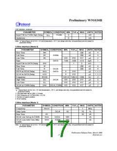
Preliminary W91030B
APPLICATION INFORMATION
Application Circuit
Analog Interface
The application circuit of the W91030B in Figure 9-1 shows the device being used within a typical
CPE system. Note that only the circuit between the W91030B and the line interface is shown. The
gain control op-amp is set to unity gain to allow the electrical characteristics to be met in this
application circuit. It should also be noted that if a glitch with sufficient amplitude appears on the tip
and ring interface, this will be detected as a ringing input by this circuit.
+5V
+5V
22nF
Tip/A
430K
34K
+5V
0.1uF
+5V
W91030B
INP
INN
VDD
ALGRC
ALGR
ALGO
INTN
+5V
10K
22nF
464K
Ring/B
430K
34K
GCFB
VREF
CAP
R1
R2
60K4
53K6
0.1uF
+5V
(This net must as short as possible)
RNGDI
RNGRC
RNGON
MODE
OSCI
FCDN
FDRN
DATA
DCLK
FSKE
+5V
0.1uF
0.1uF
470K
200K
150K
SLEEP/
RESET
TEST
OSCO
VSS
470K
0.22uF
Must rest by
microcontroller
300K
or by RC pulse.
Resistor must have 1% tolerance.
Resistor may have 5% tolerance.
R1, R2 must calculated according to the formula of Fig. 7-6 (a)
for Bellcore or BT application.
Crystal is 3.579545MHz with 0.1% frequency tolerance.
FSK 3-wire interface Mode 0 selected.
Figure 9-1 Application Circuit
Another application circuit for the W91030B, which provides common mode rejection of ringing circuit
signals, is shown in Figure 9-2. When the AC voltage between the tip and ring is greater than the
zener diode breakdown voltage, the photo-coupler LED will turn on, driving RNGDI high and thus
detecting a ringing signal. Note however in this case, a glitch on the tip and ring interface is not able
to turn on the photo-coupler and therefore will not be detected as a ringing signal.
Publication Release Date: March 2000
- 21 -
Revision A1

 WINBOND [ WINBOND ]