Preliminary W91030B
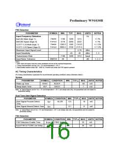
FSK Detection, continued
PARAMETER
SYMBOL CONDITION MIN.
MAX. UNITS NOTES
TYP.§
Input FSK to FCDN High Delay
FCDN
8
8
mS
CA
t
Hysteresis
mS
DD
Note: " " typical figure are at V = 5V and temperature = 25 C are design aids only, not guaranteed and not subject to
§
°
production testing.
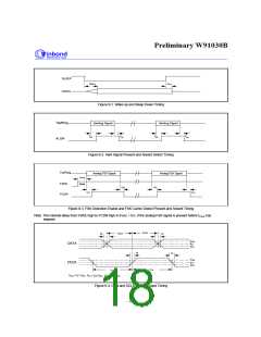
3-Wire Interface (Mode 0)
PARAMETER
Rise Time
SYMBOL CONDITION MIN.
MAX. UNITS NOTES
TYP.§
RR
t
200
200
417
1212
5
nS
nS
4
4
2
1
RF
Fall Time
t
FDRN
DATA
RL
Low Time
t
415
416
1200
1
m
S
Rate
1188
bpS
mS
nS
IDD
t
Input FSK to DATA Delay
Rise Time
R
t
200
200
4
F
Fall Time
t
DCLK
DATA
nS
4
DCD
CDD
DATA to DCLK Delay
DCLK to DATA Delay
Frequency
t
t
6
6
416
416
1, 2, 3
m
S
1, 2, 3
mS
DCLK0
f
1201.6 1202.8 1204
Hz
2
2
2
2
CH
High Time
t
DCLK
415
415
416
416
416
417
417
417
m
S
CL
Low Time
t
m
S
CRD
DCLK to FDRN Delay
t
DCLK, FDRN 415
mS
Notes:
"
" Ttypical figure are for VDD = 5V and temperature = 25 C, are design aids only, not guaranteed and not subject to
°
§
production testing.
1. FSK input data rate at 1200 +/-12 baud.
2. OSCI frequency at 3.579545 MHz +/-0.1%.
3. Function of signal condition.
4. 50 pF loading.
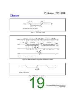
3-Wire Interface (Mode 1)
PARAMETER
Frequency
SYMBOL CONDITION MIN.
MAX. UNITS NOTES
TYP.
§
DCLK1
f
1
MHz
%
Duty Cycle
DCLK
30
70
20
R1
t
Rise Time
nS
nS
nS
DDS
DCLK Low Set-up to FDRN
t
t
DCLK,
FDRN
500
500
DDH
DCLK Low Hold Time After
FDRN
Note: " " typical figure are at VDD = 5V and temperature = 25 C are design aids only, not guaranteed and not subject to
§
°
production testing.
Publication Release Date: March 2000
Revision A1
- 17 -

 WINBOND [ WINBOND ]