Preliminary W91030B
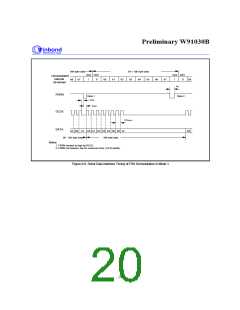
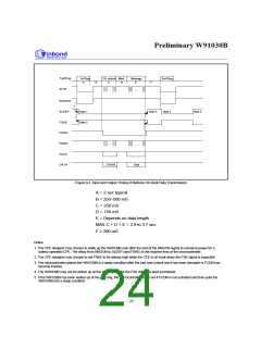
Tip/Ring
INTN
1st Ring
A
Ch. seizure Mark
Message
E
2nd Ring
B
C
D
F
...
...
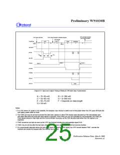
RNGON
SLEEP
FSKE
Note 1
Note 2
Note 3
Note 4
Note 5
FCDN
FDRN
DCLK
DATA
...
...
...101010...
Data
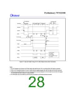
Figure 9-3. Input and Output Timing of Bellcore On-hook Data Transmission
A = 2 sec typical
-
B = 250 500 mS
C = 250 mS
D = 150 mS
E = Depends on data length
MAX C + D + E = 2.9 to 3.7 sec
³
F
200 mS
Notes:
1. The CPE designer may choose to wake up the W91030B only after the end of the RNGON signal to conserve power for a
battery operated CPE. The delay from RNGON to SLEEP (and FSKE) is the reactive time of the microcontroller.
2. The CPE designer may choose to set FSKE to be always high while the CPE is on-hook when the FSK signal is expected.
3. The microcontroller places the W91030B in a sleep condition after the last byte (check sum) has been decoded or FCDN has
become inactive.
4. The W91030B may not be woken up at this ring signal after the FSK data has been processed.
5. If the W91030B has been woken up at the 2nd ring, the microcontroller times out if FCDN is not activated and then puts the
W91030B into a sleep condition.
- 24 -

 WINBOND [ WINBOND ]