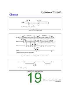
Preliminary W91030B
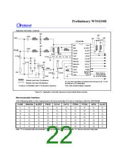
Case 1: This is the best case for microcontroller to monitor the W91030B, any condition can be
monitored.
Case 2: Analog FSK carrier detect output is not very important, FCDN pin can be ignored.
Case 3: If FSKE pin is not controlled by microcontroller, this pin must set in high state and the FSK
decode circuit is always active when W91030B is not in sleep state. The microcontroller must
take care and ignore the false data when the FSK signal is not expected.
Case 4: The FDRN pin is not very important during FSK decoding if INTN pin is used to interrupt the
microcontroller.
Case 5: If the microcontroller has no interrupt pin to use, any signal occurs of ringing, alert or byte
boundary of FSK data can not notify the microcontroller, the microcontroller must always
monitoring the RNGON, ALGO or FDRN.
Case 6: If FDRN pin can not monitored by microcontroller and the microcontroller has no interrupt pin
to use. In this case, the MODE pin must set low and the W91030B will drive DCLK pin. The
microcontroller must track the timing of DCLK pin, it is a byte boundary if DCLK high for at
least one bit width (1/1200 sec).
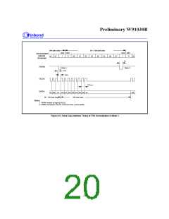
Case 7: If FDRN pin and DCLK pin can not monitored by microcontroller and the microcontroller has
no interrupt pin to use. In this case, the MODE pin must set low to set FSK data interface
mode at mode 0 and the microcontroller must track the timing of DATA pin. The DATA pin
will be toggled with 1/1200 second when FSK channel seizure input and stay in high state
when FSK mark signal input, when FSK data input, start bit (low) follows bit 0, bit 1, ...
through bit 7 then at least one bit of stop bit (high). The microcontroller must wait for the start
bit and synchronize it, acquire each bit data at proper time and check the stop bit and then
wait for next start bit arrival. The timer in the microcontroller must reset at the falling edge of
the DATA pin after stop bit has been detected.
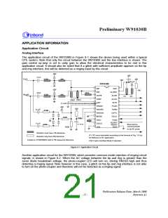
Application Environment
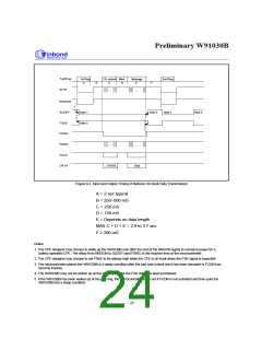
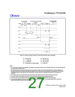
There are three major timing differences for caller ID sequences, Bellcore, BT and CCA. Figure 9-3 is
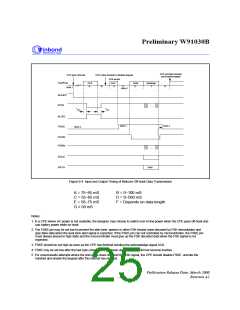
the timing diagram for the Bellcore on-hook data transmission and Figure 9-4 is the timing diagram
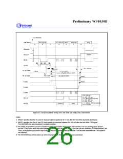
for the Bellcore off-hook data transmission. Figure 9-5 is the timing diagram for the BT caller display
service on-hook data transmission and Figure 9-6 is the timing diagram for the BT caller display
service off-hook data transmission. Figure 9-7 is the timing diagram for the CCA caller display service
for on-hook data transmission.
Publication Release Date: March 2000
- 23 -
Revision A1

 WINBOND [ WINBOND ]