W90N745CD/W90N745CDG
BITS
[31:13]
DESCRIPTION
RESERVED
-
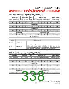
Port5 input data register
The DATAIN5 indicates the status of each GPIO17~GPIO5 pin
regardless of its operation mode. The reserved bits will be read
as 0s.
[12:0]
DATAIN5
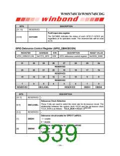
GPIO Debounce Control Register (GPIO_DBNCECON)
REGISTER
ADDRESS
R/W
DESCRIPTION
RESET VALUE
GPIO_DBNCECON
0xFFF8_3070
R/W
GPIO debounce control register 0xXXXX_XX00
31
23
15
30
29
21
13
28
27
26
18
10
2
25
17
9
24
16
8
RESERVED
22
14
6
20
12
4
19
RESERVED
11
RESERVED
3
7
5
1
0
RESERVED
DBCLKSEL
RESERVED
DBEN1
DBEN0
BITS
DESCRIPTION
[31:7]
RESERVED
-
Debounce Clock Selection
These 3 bits are used to select the clock rate for de-bouncer circuit. The
relationship between the system clock HCLK and the de-bounce clock
TCLK_BUN is as follows: TCLK_BUN = HCLK / 2DBCLKSEL
[6:4]
DBCLKSEL
[3:2]
[1]
RESERVED
-
Debounce circuit enable for GPIO17 (nIRQ1)
DBEN1
1 = enable
0 = disable
Debounce circuit enable for GPIO16 (nIRQ0)
[0]
1 = enable
0 = disable
DBEN0
- 334 -

 WINBOND [ WINBOND ]