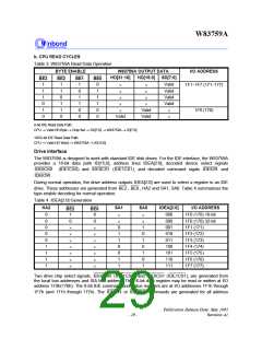
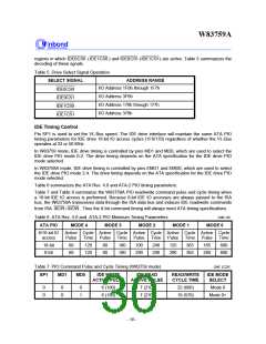
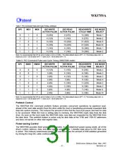
W83759A
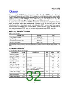
DC Characteristics, continued
PARAMETER
Operating Current
Standby Current
SYM.
IDD
CONDITIONS
FLCLK = 50 MHz
MIN.
MAX.
25
UNIT
mA
-
-
ISTBY
All input and I/O pins pulled high,
LCLK = VDD
800
mA
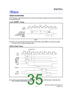
AC CHARACTERISTICS
All AC timing is measured from the 0.8V and 2.0V on the source signal to the 0.8V and 2.0V level on
the signal under test.
AC specifications are given for the following testing conditions:
VDD = 5V ± 5%, Temp. = 0° C to 70° C
VL-Bus shared signal loading = 100 pF
VL-Bus non-shared signal loading = 33 pF
ISA Bus signal loading = 240 pF
IDE device interface loading = 30 pF
SYMBOL
PARAMETER
MIN.
20
5
MAX.
UNIT
nS
FIG.
Fig. 1
t1
t2
t3
t4
LCLK Period
-
-
-
-
LCLK High Time
LCLK Low Time
nS
Fig. 1
Fig. 1
5
nS
16
LCLK Fig. 1
SYSRST Pulse Width
t5
t6
t7
t8
t9
200
10
6
-
-
-
-
nS
nS
nS
nS
nS
Fig. 1
Fig. 1
Fig. 2
Fig. 2
Fig. 2
POS Pin to SYSRST Setup Time
POS Pin Hold Time from SYSRST
LADS to LCLK Setup Time
LADS Hold Time from LCLK
3
39
LDEV Active Delay from Address
t10
t11
VESA IO Read Host Data Drive Delay
5
5
16
-
nS
nS
Fig. 2, 4
Fig. 2, 3
HMIO, HDC, HWR to LCLK Setup Time when
LDEV asserted at T2
t12
10
-
nS
Fig. 2, 3
HMIO, HDC, HWR to LCLK Setup Time when
LDEV asserted at T2
t13
t14
t15
t16
5
6
6
3
16
18
-
nS
nS
nS
nS
Fig. 2, 3
Fig. 2, 3
Fig. 2, 3
Fig. 2, 3
LRDY Active Delay from LCLK
LRDY Inactive Delay from LCLK
RDYRTN to LCLK Setup Time
-
RDYRTN Hold Time from LCLK
t17
t18
VESA IO Write Host Data Valid Delay
VESA IO Write Host Data Hold Time
-
20
-
nS
nS
Fig. 3
0
Fig. 3, 5
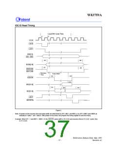
Publication Release Date: May 1995
Revision A1
- 33 -

 WINBOND [ WINBOND ]