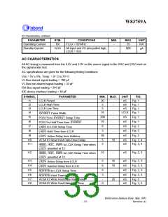
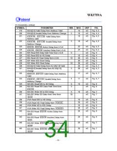
W83759A
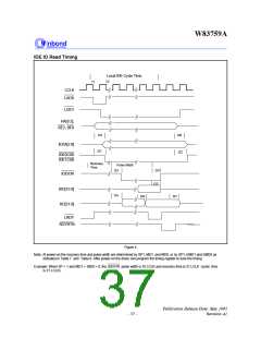
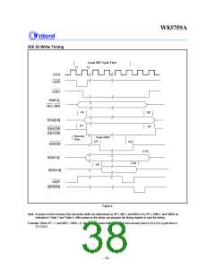
IDE IO Read Timing
Local IDE Cycle Time
T2
T1
LCLK
LADS
LDEV
HA[9:2],
BE2, BE0
t19
t21
t20
t22
IEDA[2:0]
IDE0CS0
IDE1CS0
Recovery
Time
Pulse Width
t23
t24
IDEIOR
IDD[15:0]
HD[31:0]
t25
t10
t26
t27
LRDY
RDYRTN
Figure 4
Note: At power-on the recovery time and pulse width are determined by SP1, MD1, and MD0, or by SP1, EMD1 and EMD0 as
indicated in Table 7. and Table 8. After power-on the driver can program the timing register to tune the timing.
Example: When SP = 1 and MD1 = MD0 = 0, the IDEIOR pulse width is 10 LCLK and recovery time is 21 LCLK (cycle time
is 31 LCLK).
Publication Release Date: May 1995
- 37 -
Revision A1

 WINBOND [ WINBOND ]