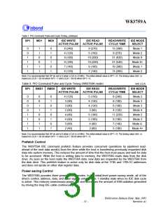
W83759A
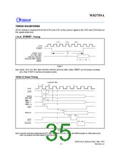
TIMING WAVEFORMS
All AC timing is measured from the 0.8V and 2.0V on the source signal to the 0.8V and 2.0V level on
the signal under test.
LCLK, SYSRST , Timing
t1
t2
t3
LCLK
SYSRST
t4
ENIDE, TEST
SP1, MD1, MD0
PRDYEN, SRDYEN
IDD[15:0], EMD1, EMD0
t5
t6
DMASL
Figure 1
Note: ENIDE, TEST, SP1, MD1, MD0, PRDYEN, SRDYEN, IDD[15:0], EMD1, EMD0, DMASL are POS (Power-On Setting)
pins. When SYSRST is low they are tri-stated as inputs.
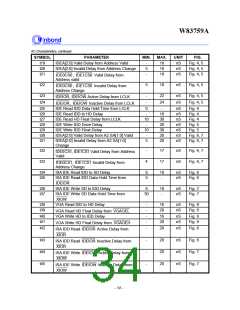
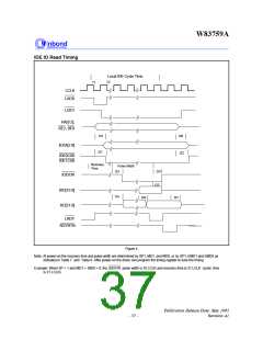
VESA IO Read Timing
Local IDE Time
T2
T1
LCLK
LADS
t8
t7
HA[9:2],
BE2, BE0
t11
t9
t12
HMIO = 0
HDC = 1
HWR = 0
LDEV
t10
HD[31:0]
t14
t13
LRDY
t15
t16
RDYRTN
Figure 2
Note: Local IDE cycle time is determined by SP1, MD1, and MD0 or by SP1, EMD1 and EMD0 at power-on. After power-on the
driver can program the timing register to tune the timing.
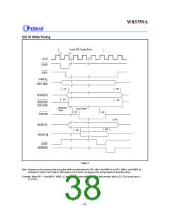
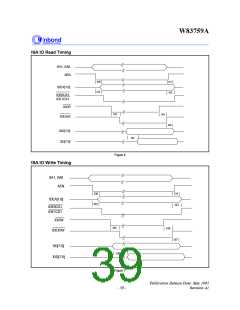
Publication Release Date: May 1995
- 35 -
Revision A1

 WINBOND [ WINBOND ]