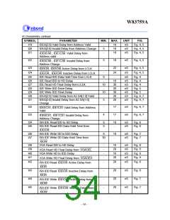
W83759A
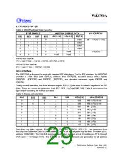
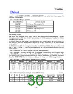
regions in which IDE0CS0 (IDE1CS0 ) and IDE0CS1 (IDE1CS1) are active. Table 5 summarizes the
decoding of these sgnals.
Table 5. Drive Select Signal Operation
SELECT SIGNAL
IDE0CS0
ADDRESS RANGE
I/O Address 1F0h through 1F7h
I/O Address 3F6h
IDE0CS1
I/O Address 170h through 177h
I/O Address 376h
IDE1CS0
IDE1CS1
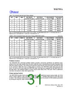
IDE Timing Control
Pin SP1 is used to set the VL-Bus speed. The IDE drive interface will maintain the same ATA PIO
timing parameters for IDE drive 16-bit IO access cycles (1F0/170) regardless of whether the VL-Bus
operates at 33 or 50 MHz.
In W83759 mode, IDE drive timing is controlled by pins MD1 and MD0, which are used to select the
IDE drive PIO mode 0-2. The drive timing depends on the ATA specification for the IDE drive PIO
mode selected.
In W83759A mode, IDE drive timing is controlled by pins EMD1 and EMD0, which are used to select
the IDE drive PIO mode 2-4. The drive timing depends on the ATA specification for the IDE drive PIO
mode selected.
Table 6 summarizes the ATA Rev. 4.0 and ATA-2 PIO timing parameters.
Table 7 and Table 8 summarize the W83759A PIO read/write command pulse and cycle timing when
a 16-bit IDE IO access is performed. Because 8-bit IDE IO accesses are always passed to the ISA
bus, the W83759A transceives data through the ISA data bus and induces IDE read/write commands
from ISA XIOR / XIOW . Thus the 8-bit command timing will always meet ATA timing specifications.
Table 6. ATA Rev. 4.0 and ATA-2 PIO Minimum Timing Parameters
ATA PIO MODE 4 MODE 3 MODE 2
8/16-bit IO Active Cycle Active Cycle Active Cycle Active Cycle Active Cycle
Unit: nS
MODE 1
MODE 0
access
16-bit
8-bit
Pulse
Time Pulse
Time
Pulse Time
Pulse Time
Pulse
Time
60
120
120
80
80
180
100
290
240
290
125
290
383
383
165
600
60
180
290
600
Table 7. PIO Command Pulse and Cycle Timing (W83759 mode)
Unit: LCLK
SP1
MD1
MD0
IDE WRITE
ACTIVE PULSE
IDE READ
ACTIVE PULSE
READ/WRITE
CYCLE TIME
IDE MODE
SELECT
0
0
0
0
0
1
6 (180)
6 (180)
7 (210)
7 (210)
22 (660)
19 (570)
Mode 0
Mode 0+
- 30 -

 WINBOND [ WINBOND ]