W83759A
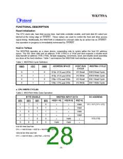
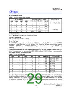
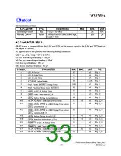
b. CPU READ CYCLES
Table 3. W83759A Read Data Operation
BYTE ENABLE
W83759A OUTPUT DATA
HD[31:16] HD[15:0] SD[7:0]
I/O ADDRESS
BE3
1
BE2
1
BE1
1
BE0
0
Valid
Valid
Valid
Valid
´
´
´
1F1- 1F7 (171- 177)
1
1
0
1
´
´
1
0
1
1
´
´
0
1
1
1
´
´
´
1
1
0
0
Valid
Valid
1F0 (170)
0
0
0
0
Valid
´
8-bit IDE Read Data Path:
CPU ® Valid HD Byte ® Chip Set ® SD[7:0] ® W83759A ® ID[7:0]
16/32-bit IDE Read Data Path:
CPU ® Valid HD Word ® W83759A ® ID[15:0]
Drive Interface
The W83759A is designed to work with standard IDE disk drives. For the IDE interface, the W83759A
provides a 16-bit data path ID[15;0], address lines IDEA[2:0], decoded device select signals
IDE0CS0
IDEIOW .
(IDE1CS0) and IDE0CS1 (IDE1CS1), and decoded command sigals IDEIOR and
During normal operation, the drive address outputs IDEA[2:0] are used to select a register in an IDE
drive. These addresses are generated from BE2 , BE0 , HA2 and SA1, SA0. Table 4 summarizes the
type enable decoding for normal operation.
Table 4. IDEA[2:0] Generation
HA2
0
SA1
SA0
IDEA[2:0]
000
I/O ADDRESS
1F0 (170) 16-bit
1F0 (170) 32-bit
1F1 (171)
BE2
1
BE0
0
´
´
0
0
0
000
´
´
0
0
1
1
0
0
1
1
1
0
1
0
1
0
1
001
´
´
´
´
´
´
´
´
´
´
´
´
´
´
0
010
1F2 (172)
0
011
1F3 (173)
1
100
1F4 (174)
1
101
1F5 (175)
1
110
1F6 (176)
1
111
1F7 (177)
Two drive chip select signals, IDE0CS0 (IDE1CS0 ) and IDE0CS1 (IDE1CS1), are generated from
the local bus addresses and ISA bus address. The 16-bit data register may be read or written at I/O
address 1F0h(170h). The 8-bit IDE command and status registers are at I/O addresses 1F1h through
1F7h (and 171h through 177h). The IDEIOR or IDEIOW commands are generated for all address
Publication Release Date: May 1995
- 29 -
Revision A1

 WINBOND [ WINBOND ]