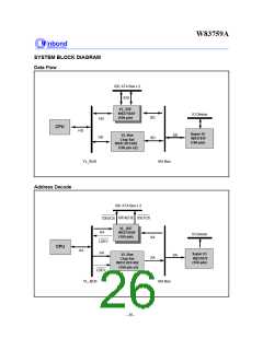
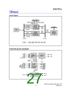
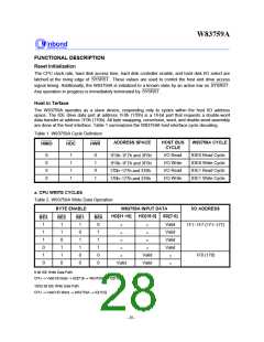
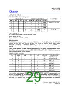
W83759A
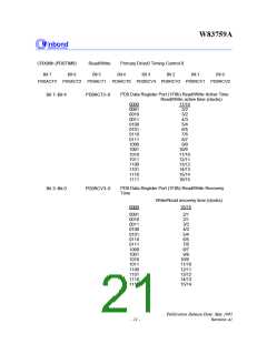
CRX8Eh (SD1TIM0)
Bit 7 Bit 6
Read/Write
Bit 5
Secondary Drive 1 Timing Control 0
Bit 4 Bit 3 Bit 2
Bit 1
Bit 0
SD1ACT3 SD1ACT2 SD1ACT1 SD1ACT0 SD1RCV3 SD1RCV2 SD1RCV1 SD1RCV0
SD1 Data Register Port (170h) Read/Write Active Time
Definition of these bits same as PD0RCV3-0
Bit 7- Bit 4
Bit 3- Bit 0
SD1ACT3- 0
SD1RCV3- 0
SD1 Data Register Port (170h) Read/Write Recovery Time
Definition of these bits same as PD0RCV3-0
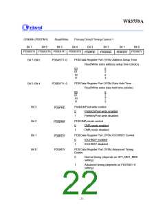
CRX8Fh (SD1TIM1)
Read/Write
Secondary Drive 1 Timing Control 1
Bit 7
Bit 6
Bit 5
Bit 4
Bit 3
Bit 2
Bit 1
Bit 0
SD1AST1
SD1AST0
SD1DHT1
SD1DHT0
SD1ADV
SD1PRE
SD1DMA
SD1RDY
SD1 Data Register Port (170h) Address Setup Time
Bit 7- Bit 6
SD1AST1- 0
SD1DHT1- 0
Definition of these bits same as PD0RCV3- 0
SD1 Data Register Port (170h) Data Hold Time
Bit 5- Bit 4
Definition of these bits same as PD0RCV3- 0
Bit 3
SD1 Prefetch/Post write control
SD1PRE
SD1DMA
0
1
Prefetch/Post write enabled
Prefetch/Post write disabled
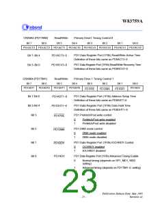
Bit 2
Bit 1
Bit 0
SD1 DMA mode control
0
1
DMA mode enabled
DMA mode disabled
SD1 Data Register Port (170h) IOCHRDY Control
SD1RDY
SD1ADV
0
1
IOCHRDY enabled
OCHRDY disabled
SD1 Data Register Port (170h) Advanced Timing Enable
0
Normal timing (depends on SP1, MD1, MD0
setting)
1
Advanced timing (depends on SD1TIM1- 0 setting)
Publication Release Date: May 1995
- 25 -
Revision A1

 WINBOND [ WINBOND ]