Preliminary W78E378/W78C378/W78C374
a) Control Registers
a-1) The Address Registers, S1ADR1, S1ADR2
The SIO1 is equipped with two address registers: S1ADR1 & S1ADR2. The CPU can read from and
write to these two 8-bit, directly addressable SFRs. The content of these registers are irrelevant when
SIO1 is in master modes. In the slave modes, the seven most significant bits must be loaded with the
MCU's own address. The SIO1 hardware will react if either of the addresses is matched.
7
6
5
4
3
2
1
0
-
X
X
X
X
X
X
X
|------------------------ Own Slave Address -----------------------|
a-2) The Data Register, S1DAT
This register contains a byte of serial data to be transmitted or a byte which has just been received.
The CPU can read from or write to this 8-bit directly addressable SFR while it is not in the process of
shifting a byte. This occurs when SIO1 is in a defined state and the serial interrupt flag (SI) is set.
Data in S1DAT remains stable as long as SI is set. While data is being shifted out, data on the bus is
simultaneously being shifted in; S1DAT always contains the last data byte present on the bus. Thus,
in the event of lost arbitration, the transition from master transmitter to slave receiver is made with
the correct data in S1DAT.
7
6
5
4
3
2
1
0
SD7
SD6
SD5
SD4
SD3
SD2
SD1
SD0
|<---------------------------- Shift direction -----------------------------
S1DAT and the acknowledge bit form a 9-bit shift register, the acknowledge bit is controlled by the
SIO1 hardware and cannot be accessed by the CPU. Serial data is shifted through the acknowledge
bit into S1DAT on the rising edges of serial clock pulses on the SCL line. When a byte has been
shifted into S1DAT, the serial data is available in S1DAT, and the acknowledge bit (ACK or NACK) is
returned by the control logic during the ninth clock pulse. Serial data is shifted out from S1DAT on the
falling edges of SCL clock pulses, and is shifted into S1DAT on the rising edges of SCL clock pulses.
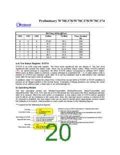
a-3) The Control Register, S1CON
The CPU can read from and write to this 8-bit, directly addressable SFR. Two bits are affected by the
SIO1 hardware: the SI bit is set when a serial interrupt is requested, and the STO bit is cleared when
a STOP condition is present on the bus. The STO bit is also cleared when ENS1 = "0".
7
6
5
4
3
2
1
0
CR2
ENS1
STA
STO
SI
AA
CR1
CR0
ENS1, the SIO1 Enable Bit
ENS1 = "0": When ENS1 is "0", the SDA and SCL outputs are in a high impedance state. SDA and
SCL input signals are ignored, SIO1 is in the not addressed slave state, and STO bit in S1CON is
forced to "0". No other bits are affected. P3.0 (SDA) and P3.1 (SCL) may be used as open drain I/O
ports.
ENS1 = "1": When ENS1 is "1", SIO1 is enabled. The P3.0 and P3.1 port latches must be set to logic
1.
- 18 -

 WINBOND [ WINBOND ]