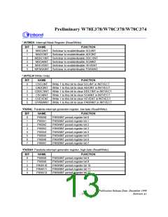
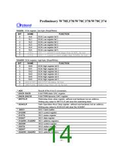
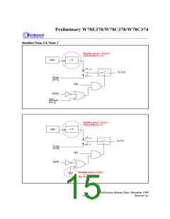
Preliminary W78E378/W78C378/W78C374
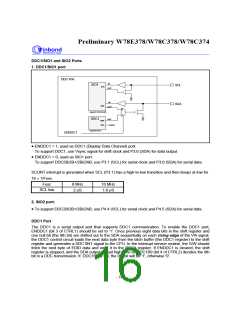
To use DDC1 port, a user should pay attention to the following items:
(1) When the chip is powered-on or after reset , the 8-bit shift register in DDC1 H/W contains all 0s. If
you write a data to the latch buffer (the DDC1 register), it will be loaded to the shift register at the
IN
9th clock (on V ), so from the 10th clock, the real data bit begins to shift out.
(2) Because there is no reset signal to the latch buffer, it contains a random data after power-on. If
you enable DDC1 without writing data to the latch buffer, SDA will have the random data shifted
out after 9 clocks. The shift register is reset to 00H during CPU reset.
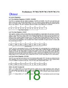
(3) The DDC1 H/W has a counter that counts how many bits shifted out. This counter is initialized to 0
when power-up or reset. When you firstly enable DDC1 after power-on, the first bit is already
shifted out without clock, so the first clock triggers the second data bit (D6) to shift out and "0000
0001 1" will be got. After the first 9 clocks that shift out an invalid byte, the counter counts from 1
IN
to 9 cyclically according to the clock pulse on V -pin. See the following illustration.
0 1 2 3 4 5 6 7 8 9
1
2
3
4
5
6
7
8
9
1
2
3
4
5
6
7
8
9
...
After power on, the
counter count:
0 0 0 0 0 0 0 0 1 1 D7 D6 D5 D4 D3 D2 D1 D0 ack D7 D6 D5 D4 D3 D2 D1 D0 ack
…
shifted-out data bit:
1 2 3 4 5 6 7 8 9
|--> invalid data
1
2
3
4
5
6
7
8
9
1
2
3
4
5
6
7
8
9
...
IN
V
clock pulse:
|--> normal data
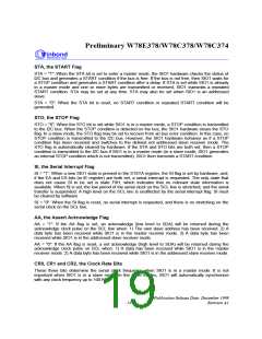
(4) The interrupt happens on the failing edge of the following first clock. The next data, which is about
to be shifted out, in the latch buffer is loaded into the shift register at the rising edge of the
following first clock. At the same time, data bit D7 is shifted out and the counter value is "1".
SIO1 Port (with two slave addresses)
The SIO1 port is a serial I/O port, which supports all transfer modes from and to the I2C bus. The
SIO1 port handles byte transfers autonomously. To enable this port, the bit ENDDC1 in CTRL1
should be cleared to '0'. The CPU interfaces to the SIO1 port through the following five special
S1CON
S1ADR1 S1ADR2
S1STA
S1DAT
function registers:
register, DAh) and
(control register, D8h),
(status register, D9h), (data
/
(address registers, DBh/DCh). The SIO1 H/W interfaces to the
I2C bus via two pins: SDA (P3.0, serial clock line) and SCL (P3.1, serial data line). The output latches
of P3.0 and P3.1 must be set to "1" before using this port.
SIO2 Port (with two slave addresses)
The function of this port is the same as SIO1 port. The CPU interfaces to the SIO2 port through the
S2CON
S2STA
following five special function registers:
(control register, E8h),
(status register, E9h),
S2DAT
S2ADR1 S2ADR2
(data register, EAh) and
/ (address registers, EBh/ECh). The SIO2 H/W
interfaces to the I2C bus via two pins: SDA2 (P4.5, serial clock line) and SCL2 (P4.4, serial data line).
The output latches of P4.5 and P4.4 must be set to "1" before using this port.
Operation of SIO1 Port:
(SIO2 has the same function except their addresses of control registers)
Publication Release Date: December 1999
- 17 -
Revision A1

 WINBOND [ WINBOND ]