W25X10BV/20BV/40BV
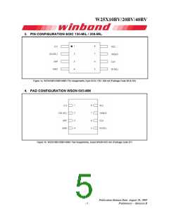
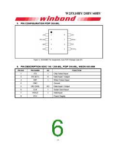
6.1
Package Types
W25X10BV/20BV/40BV are offered in an 8-pin plastic 150-mil width SOIC (package code SN) and
6x5-mm WSON (package code ZP), see figures 1a and 1b, respectively. The W25X40BV is offered in
the 208-mil width SOIC (package code SS) and the 300-mil 8-pin PDIP (package code DA), see figure
1c. Package diagrams and dimensions are illustrated at the end of this datasheet.
6.2 Chip Select (/CS)
The SPI Chip Select (/CS) pin enables and disables device operation. When /CS is high the device is
deselected and the Serial Data Output (DO) pin is at high impedance. When deselected, the devices
power consumption will be at standby levels unless an internal erase, program or status register cycle
is in progress. When /CS is brought low the device will be selected, power consumption will increase
to active levels and instructions can be written to and data read from the device. After power-up, /CS
must transition from high to low before a new instruction will be accepted. The /CS input must track
the VCC supply level at power-up (see “Write Protection” and Figure 25). If needed a pull-up resister
on /CS can be used to accomplish this.
6.3 Serial Data Input, Output and IOs (DI, DO, IO0 and IO1)
The W25X10BV/20BV/40BV supports standard SPI and Dual SPI operation. Standard SPI instructions
use the unidirectional DI (input) pin to serially write instructions, addresses or data to the device on the
rising edge of the Serial Clock (CLK) input pin. Standard SPI also uses the unidirectional DO (output)
to read data or status from the device on the falling edge of CLK.
Dual SPI instructions use the bidirectional IO pins to serially write instructions, addresses or data to
the device on the rising edge of CLK and read data or status from the device on the falling edge of
CLK.
6.4 Write Protect (/WP)
The Write Protect (/WP) pin can be used to prevent the Status Register from being written. Used in
conjunction with the Status Register’s Block Protect (BP2, BP1, and BP0) bits and Status Register
Protect (SRP) bit, a portion or the entire memory array can be hardware protected. The /WP pin is
active low.
6.5 HOLD (/HOLD)
The Hold (/HOLD) pin allows the device to be paused while it is actively selected. When /HOLD is
brought low, while /CS is low, the DO pin will be at high impedance and signals on the DIO and CLK
pins will be ignored (don’t care). When /HOLD is brought high, device operation can resume. The
/HOLD function can be useful when multiple devices are sharing the same SPI signals. (“See Hold
function”)
6.6 Serial Clock (CLK)
The SPI Serial Clock Input (CLK) pin provides the timing for serial input and output operations. (“See
SPI Operations”)
Publication Release Date: August 20, 2009
- 7 -
Preliminary -- Revision B

 WINBOND [ WINBOND ]