W25X10BV/20BV/40BV
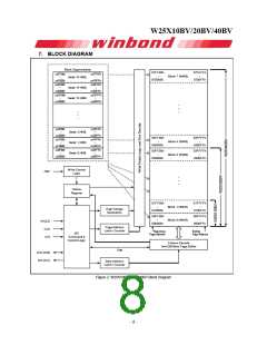
8.
FUNCTIONAL DESCRIPTION
8.1 SPI OPERATIONS
8.1.1 Standard SPI Instructions
The W25X10BV/20BV/40BV are accessed through an SPI compatible bus consisting of four signals:
Serial Clock (CLK), Chip Select (/CS), Serial Data Input (DI) and Serial Data Output (DO). Standard
SPI instructions use the DI input pin to serially write instructions, addresses or data to the device on
the rising edge of CLK. The DO output pin is used to read data or status from the device on the falling
edge CLK.
SPI bus operation Modes 0 (0,0) and 3 (1,1) are supported. The primary difference between Mode 0
and Mode 3 concerns the normal state of the CLK signal when the SPI bus master is in standby and
data is not being transferred to the Serial Flash. For Mode 0 the CLK signal is normally low on the
falling and rising edges of /CS. For Mode 3 the CLK signal is normally high on the falling and rising
edges of /CS..
8.1.2 Dual SPI Instructions
The W25X10BV/20BV/40BV supports Dual SPI operation when using the “Fast Read Dual Output
(3Bh)” and “Fast Read Dual I/O (BBh)” instructions. These instructions allow data to be transferred to
or from the device at two to three times the rate of ordinary Serial Flash devices. The Dual SPI Read
instructions are ideal for quickly downloading code to RAM upon power-up (code-shadowing) or for
executing non-speed-critical code directly from the SPI bus (XIP). When using Dual SPI instructions,
the DI and DO pins become bidirectional I/O pins: IO0 and IO1.
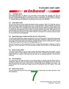
8.1.3 Hold Function
The /HOLD signal allows the W25X10BV/20BV/40BV operation to be paused while it is actively
selected (when /CS is low). The /HOLD function may be useful in cases where the SPI data and clock
signals are shared with other devices. For example, consider if the page buffer was only partially
written when a priority interrupt requires use of the SPI bus. In this case the /HOLD function can save
the state of the instruction and the data in the buffer so programming can resume where it left off once
the bus is available again.
To initiate a /HOLD condition, the device must be selected with /CS low. A /HOLD condition will
activate on the falling edge of the /HOLD signal if the CLK signal is already low. If the CLK is not
already low the /HOLD condition will activate after the next falling edge of CLK. The /HOLD condition
will terminate on the rising edge of the /HOLD signal if the CLK signal is already low. If the CLK is not
already low the /HOLD condition will terminate after the next falling edge of CLK.
During a /HOLD condition, the Serial Data Output (DO) is high impedance, and Serial Data
Input/Output (DIO) and Serial Clock (CLK) are ignored. The Chip Select (/CS) signal should be kept
active (low) for the full duration of the /HOLD operation to avoid resetting the internal logic state of the
device.
Publication Release Date: August 20, 2009
- 9 -
Preliminary -- Revision B

 WINBOND [ WINBOND ]