W25X10BV/20BV/40BV
8.2 WRITE PROTECTION
Applications that use non-volatile memory must take into consideration the possibility of noise and
other adverse system conditions that may compromise data integrity. To address this concern the
W25X10BV/20BV/40BV provides several means to protect data from inadvertent writes.
8.2.1 Write Protect Features
Device resets when VCC is below threshold.
Time delay write disable after Power-up.
Write enable/disable instructions.
Automatic write disable after program and erase.
Software write protection using Status Register.
Hardware write protection using Status Register and /WP pin.
Write Protection using Power-down instruction.
Upon power-up or at power-down the W25X10BV/20BV/40BV will maintain a reset condition while
VCC is below the threshold value of VWI, (See Power-up Timing and Voltage Levels and Figure 25).
While reset, all operations are disabled and no instructions are recognized. During power-up and after
the VCC voltage exceeds VWI, all program and erase related instructions are further disabled for a
time delay of tPUW. This includes the Write Enable, Page Program, Sector Erase, Block Erase, Chip
Erase and the Write Status Register instructions. Note that the chip select pin (/CS) must track the
VCC supply level at power-up until the VCC-min level and tVSL time delay is reached. If needed a pull-
up resister on /CS can be used to accomplish this.
After power-up the device is automatically placed in a write-disabled state with the Status Register
Write Enable Latch (WEL) set to a 0. A Write Enable instruction must be issued before a Page
Program, Sector Erase, Chip Erase or Write Status Register instruction will be accepted. After
completing a program, erase or write instruction the Write Enable Latch (WEL) is automatically
cleared to a write-disabled state of 0.
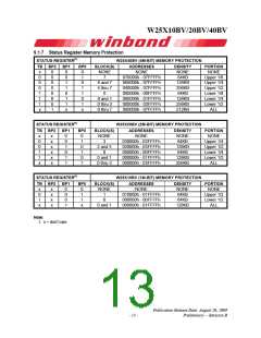
Software controlled write protection is facilitated using the Write Status Register instruction and setting
the Status Register Protect (SRP) and Block Protect (TB, BP2, BP1, and BP0) bits. These Status
Register bits allow a portion or all of the memory to be configured as read only. Used in conjunction
with the Write Protect (/WP) pin, changes to the Status Register can be enabled or disabled under
hardware control. See Status Register for further information.
Additionally, the Power-down instruction offers an extra level of write protection as all instructions are
ignored except for the Release Power-down instruction.
- 10 -

 WINBOND [ WINBOND ]