W25X10BV/20BV/40BV
1. GENERAL DESCRIPTION
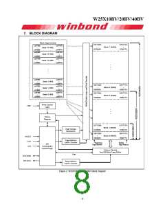
The W25X10BV (1M-bit), W25X20BV (2M-bit) and the W25X40BV (4M-bit) Serial Flash memories
provides a storage solution for systems with limited space, pins and power. The 25X series offers
flexibility and performance well beyond ordinary Serial Flash devices. They are ideal for code
download applications as well as storing voice, text and data. The devices operate on a single 2.7V to
3.6V power supply with current consumption as low as 4mA active and 1µA for power-down. All
devices are offered in space-saving packages.
The W25X10BV/20BV/40BV arrays are organized into 512/1,024/2,048 programmable pages of 256-
bytes each. Up to 256 bytes can be programmed at a time using the Page Program instruction. Pages
can be erased in groups of 16 (sector erase), groups of 128 (32KB block erase), groups of 256 (block
erase) or the entire chip (chip erase). The W25X10BV/20BV/40BV has 32/64/128 erasable sectors
and 2/4/8 erasable 64KB blocks respectively. The small 4KB sectors allow for greater flexibility in
applications that require data and parameter storage. (See figure 2.)
The W25X10BV/20BV/40BV supports the standard Serial Peripheral Interface (SPI), and a high
performance dual output as well as Dual I/O SPI: Serial Clock, Chip Select, Serial Data DI (I/O0), DO
(I/O1). SPI clock frequencies of up to 104MHz are supported allowing equivalent clock rates of
208MHz when using the Fast Read Dual Output instruction. These transfer rates are comparable to
those of 8 and 16-bit Parallel Flash memories.
A Hold pin, Write Protect pin and programmable write protect, with top or bottom array control
features, provide further control flexibility. Additionally, the device supports JEDEC standard
manufacturer and device identification.
2. FEATURES
Software and Hardware Write Protection
– Write-Protect all or portion of memory
– Enable/Disable protection with /WP pin
– Top or bottom array protection
Family of Serial Flash Memories
– W25X10BV: 1M-bit/128K-byte (131,072)
– W25X20BV: 2M-bit/256K-byte (262,144)
– W25X40BV: 4M-bit/512K-byte (524,288)
– 256-bytes per programmable page
Flexible Architecture with 4KB sectors
– Sector Erase (4K-bytes)
– Uniform 4KB Sectors, 32KB & 64KB Blocks
– Block Erase (32K and 64K-byte)
– Page program up to 256 bytes <1ms
– More than 100,000 erase/write cycles
– More than 20-year retention
SPI with Single / Dual Outputs / Dual I/O
– Clock, Chip Select, Data I/O, Data Out
– Optional Hold function for SPI flexibility
Data Transfer up to 208M-bits / second
– Clock operation to 104MHz
– Fast Read Dual Output instruction
– Auto-increment Read capability
Low Power Consumption, Wide
Temperature Range
– Single 2.7 to 3.6V supply
– 4mA active current, 1µA Power-down (typ)
– -40° to +85°C operating range
Efficient “Continuous Read Mode”
– Low Instruction overhead
– Continuous Read
– As few as 8 clocks to address memory
– Allows true XIP (execute in place) operation
Space Efficient Packaging
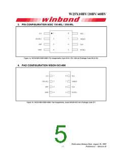
– 8-pin SOIC 150-mil
– 8-pin SOIC 208-mil
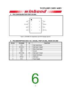
– 8-pad WSON 6x5-mm
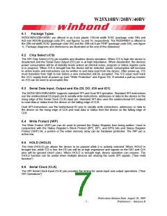
– 8-pin PDIP 300-mil
- 4 -

 WINBOND [ WINBOND ]