WED3DL644V
White Electronic Designs
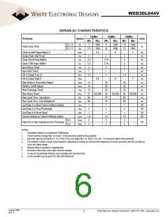
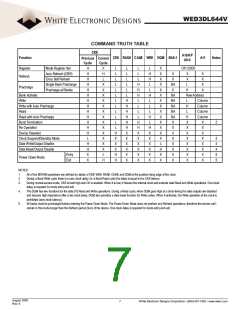
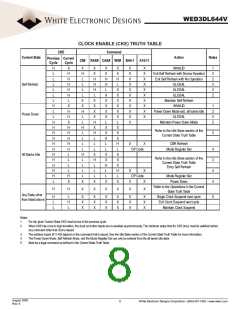
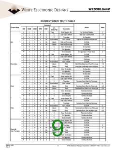
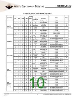
COMMAND TRUTH TABLE
CKE
A10/AP
Function
CE# RAS# CAS# WE# DQM BA0-1
A11
Notes
Previous Current
Cycle
H
A9-0
Cycle
X
H
L
X
X
X
X
X
X
X
X
X
X
X
X
X
L
Register
Refresh
Mode Register Set
Auto Refresh (CBR)
Entry Self Refresh
Single Bank Precharge
Precharge all Banks
L
L
L
L
L
L
L
L
L
L
L
L
H
X
X
X
H
H
L
L
L
L
L
L
L
L
H
H
H
L
L
L
L
H
H
X
X
X
X
X
X
L
H
H
L
L
H
L
L
L
H
L
H
X
X
X
X
X
X
X
X
X
X
X
X
X
X
X
X
X
X
X
X
L
OP CODE
H
H
H
H
H
H
H
H
H
H
H
H
L
H
H
X
X
X
BA
X
BA
BA
BA
BA
BA
X
X
X
X
X
X
X
X
X
X
L
X
X
X
X
Precharge
H
Bank Activate
Write
Write with Auto Precharge
Read
L
Row Address
H
H
H
H
H
H
X
X
X
X
X
X
L
H
L
Column
Column
Column
Column
X
X
X
X
X
X
X
X
Read with Auto Precharge
Burst Termination
H
X
X
X
X
X
X
X
X
2
No Operation
Device Deselect
Clock Suspend/Standby Mode
Data Write/Output Disable
Data Mask/Output Disable
3
4
4
5
5
H
X
X
Entry
Exit
Power Down Mode
X
H
NOTES:
1.
2.
3.
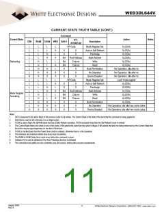
All of the SDRAM operations are defined by states of CE#, WE#, RAS#, CAS#, and DQM at the positive rising edge of the clock.
During a Burst Write cycle there is a zero clock delay, for a Burst Read cycle the delay is equal to the CAS latency.
During normal access mode, CKE is held high and CK is enabled. When it is low, it freezes the internal clock and extends data Read and Write operations. One clock
delay is required for mode entry and exit.
The DQM has two functions for the data DQ Read and Write operations. During a Read cycle, when DQM goes high at a clock timing the data outputs are disabled
and become high impedance after a two clock delay. DQM also provides a data mask function for Write cycles. When it activates, the Write operation at the clock is
prohibited (zero clock latency).
4.
5.
All banks must be precharged before entering the Power Down Mode. The Power Down Mode does not preform any Refresh operations, therefore the device can’t
remain in this mode longer than the Refresh period (tREF) of the device. One clock delay is required for mode entry and exit.
August 2005
Rev. 6
7
White Electronic Designs Corporation • (602) 437-1520 • www.wedc.com

 WEDC [ WHITE ELECTRONIC DESIGNS CORPORATION ]