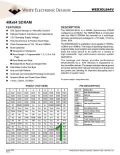
WED3DL644V
White Electronic Designs
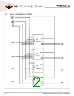
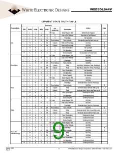
INPUT/OUTPUT FUNCTIONAL DESCRIPTION
Symbol
Type
Signal
Polarity
Function
The system clock input. All of the SDRAM inputs are sampled on the rising edge of the
clock.
CK
Input
Pulse
Positive Edge
Activates the CK signal when high and deactivates the CK signal when low. By
CKE
Input
Input
Level
Pulse
Active High deactivating the clock, CKE low initiates the Power Down mode, Suspend mode, or the
Self Refresh mode.
CE# disable or enable device operation by masking or enabling all inputs except CK,
CKE and DQM.
CE#
Active Low
RAS#, CAS#
WE#
BA0,BA1
When sampled at the positive rising edge of the clock, CAS#, RAS#, and WE# define the
Input
Input
Pulse
Level
Active Low
operation to be executed by the SDRAM.
—
—
Selects which SDRAM bank is to be active.
During a Bank Activate command cycle, A0-11 defines the row address (RA0-11) when
sampled at the rising clock edge.
During a Read or Write command cycle, A0-7 defines the column address (CA0-7) when
sampled at the rising clock edge. In addition to the row address, A10/AP is used to invoke
Autoprecharge operation at the end of the Burst Read or Write cycle. If A10/AP is high,
autoprecharge is selected and BA0, BA1 defines the bank to be precharged. If A10/AP is
low, autoprecharge is disabled.
A0-11,
A10/AP
Input
Level
During a Precharge command cycle, A10/AP is used in conjunction with BA0, BA1
to control which bank(s) to precharge. If A10/AP is high, all banks will be precharged
regardless of the state of BA0, BA1. If A10/AP is low, then BA0, BA1 is used to define
which bank to precharge.
DQ
Input/Output
Input
Level
Pulse
—
Data Input/Output are multiplexed on the same pins
DQML0 - (DQ0-7)
DQMH0 - (DQ8-15)
DQML1 - (DQ16-23)
DQMH1 - (DQ24-31)
DQML2 - (DQ31-39)
DQMH2 - (DQ40-47)
DQML3 - (DQ48-55)
DQMH3 - (DQ56-63)
The Data Input/Output mask places the DQ buffers in a high impedance state when
sampled high. In Read mode, DQM has a latency of two clock cycles and controls
the output buffers like an output enable. In Write mode, DQM has a latency of zero
Mask
Active High and operates as a word mask by allowing input data to be written if it is low but blocks
the Write operation if DQM is high. Each DQM pin controls the byte in parentheses
associated with it.
V
CC, VSS
Supply
Power and ground.
ABSOLUTE MAXIMUM RATINGS
RECOMMENDED DC OPERATING CONDITIONS
(Voltage Referenced to: Vss = 0V)
Parameter
Symbol
VCC/VCCQ
VIN
VOUT
tOPR
tSTG
PD
IOS
Min
-1.0
-1.0
-1.0
-40
-55
—
Max
+4.6
+4.6
+4.6
+85
+125
3.0
Units
V
V
Parameter
Supply Voltage
Symbol Min Typ
VCC/VCCQ 3.0 3.3
Max
3.6
Unit
V
Power Supply Voltage
Input Voltage
Output Voltage
Operating Temperature
Storage Temperature
Power Dissipation
Short Circuit Output Current
Input High Voltage
Input Low Voltage
Output High Voltage (IOH =-2mA)
Output Low Voltage (IOL = 2mA)
Input Leakage Voltage
Output Leakage Voltage
VIH
VIL
VOH
VOL
IIL
2.0 3.0 VCC +0.3
V
V
V
V
µA
µA
V
-0.3
2.4
—
—
—
—
—
—
0.8
—
0.4
5
°C
°C
W
-5
—
50
mA
IOL
-5
5
Stress greater than those listed under “Absolute Maximum Ratings” may cause
permanent damage to the device. This is a stress rating only and functional operation
of the device at these or any other conditions greater than those indicated in the
operational sections of this specification is not implied. Exposure to absolute maximum
rating conditions for extended periods may affect reliability.
CAPACITANCE
(TA = 25°C, f= 1MHZ, VCC = 3.3V)
Parameter
Input Capacitance
Symbol
CIN
Max
8
5
Unit
pF
pF
Input/Output Capacitance (DQ)
COUT
August 2005
Rev. 6
3
White Electronic Designs Corporation • (602) 437-1520 • www.wedc.com

 WEDC [ WHITE ELECTRONIC DESIGNS CORPORATION ]