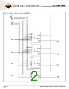
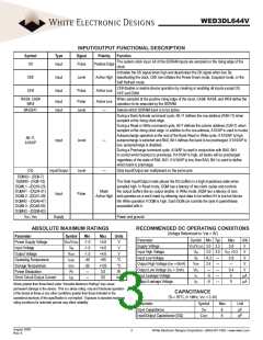
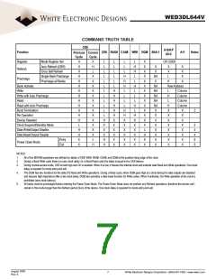
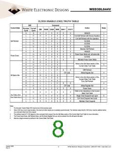
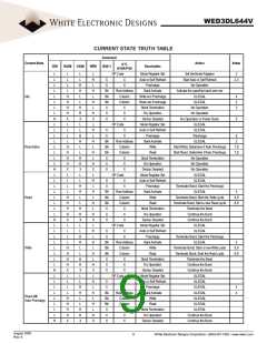
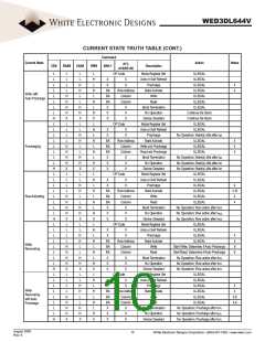
WED3DL644V
White Electronic Designs
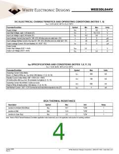
SDRAM AC CHARACTERISTICS
133MHZ
125MHZ
100MHZ
Parameter
Symbol
Units
Min
Max
1000
1000
5.4
Min
8
Max
1000
1000
6
Min
10
12
Max
1000
1000
7
CL = 3
CL = 2
tCC
tCC
tSAC
tOH
tCH
tCL
7
Clock Cycle Time1
ns
7.5
10
Clock to valid Output delay1,2
Output Data Hold Time2
Clock HIGH Pulse Width3
Clock LOW Pulse Width3
Input Setup Time3
Input Hold Time3
CK to Output Low-Z2
CK to Output High-Z
Row Active to Row Active Delay4
RAS# to CAS# Delay4
ns
ns
ns
ns
ns
ns
ns
ns
ns
ns
ns
ns
ns
ns
CK
CK
CK
CK
2
2.5
2.5
2
2
2.75
2.75
2
2
3
3
2
1
tSS
tSH
1
1
1
tSLZ
tSHZ
tRRD
tRCD
tRP
1.0
1.5
5.4
6
7
14
15
15
20
20
20
20
20
20
Row Precharge Time4
Row Active Time4
tRAS
tRC
37 120,000 50
120,000
50 120,000
Row Cycle Time - Operation4
Row Cycle Time - Auto Refresh4,8
Last Data in to New Column Address Delay5
Last Data in to Row Precharge5
Last Data in to Burst Stop5
Column Address to Column Address Delay6
60
66
1
70
70
1
2
1
80
80
1
tRFC
tCDL
tRDL
tBDL
tCCD
tROH
tROH
2
1
2
1
1.0
3
1.0
3
1.5
3
CL3
CL2
Data Out to High Impedance from Precharge
CK
2
2
2
NOTES:
1.
2.
3.
4.
Parameters depend on programmed CAS# latency.
If clock rise time is longer than 1ns (tRISE/2 -0.5)ns should be added to the parameter.
Assumed input rise and fall time = 1ns. If tRISE of tFALL are longer than 1ns. [(tRISE = tFALL)/2] - 1ns should be added to the parameter.
The minimum number of clock cycles required is detemined by dividing the minimum time required by the clock cycle time and then rounding up
to the next higher integer.
Minimum delay is required to complete write.
All devices allow every cycle column address changes.
5.
6.
7.
8.
In case of row precharge interrupt, auto precharge and read burst stop.
A new command may be given tRFC after self-refresh exit
August 2005
Rev. 6
6
White Electronic Designs Corporation • (602) 437-1520 • www.wedc.com

 WEDC [ WHITE ELECTRONIC DESIGNS CORPORATION ]