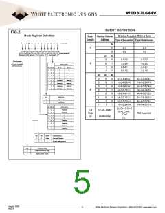
WED3DL644V
White Electronic Designs
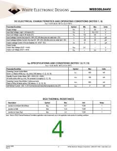
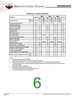
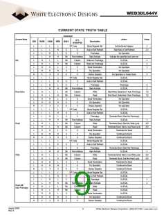
DC ELECTRICAL CHARACTERISTICS AND OPERATING CONDITIONS (NOTES 1, 6)
VCC = +3.3V 0.3V; -55°C ≤ TA ≤ +125°C
Parameter/Condition
Supply Voltage
Input High Voltage: Logic 1; All inputs (21)
Input Low Voltage: Logic 0; All inputs (21)
Input Leakage Current: Any input 0V VIN VCC (All other pins not under test = 0V)
Input Leakage Address Current: Any input 0V VIN VCC (All other pins not under test = 0V)
Output Leakage Current: I/Os are disabled; 0V VOUT VCC
Symbol
Min
3
2
-0.3
-5
-20
-5
Max
3.6
VCC + 0.3
0.8
5
Units
V
V
VCC
VIH
VIL
II
II
IOZ
V
µA
µA
µA
20
5
Output Levels:
Output High Voltage (IOUT = -4mA)
Output Low Voltage (IOUT = 4mA)
VOH
VOL
2.4
–
–
0.4
V
V
IDD SPECIFICATIONS AND CONDITIONS (NOTES 1,6,11,13)
VCC = +3.3V 0.3V; -55°C ≤ TA ≤ 125°C
Parameter/Condition
Symbol
Max
Units
Operating Current: Active Mode;
ICC1
460
180
mA
mA
Burst = 2; Read or Write; tRC = tRC (min); CAS latency = 3 (3, 18, 19)
Standby Current: Active Mode; CKE = HIGH; CS = HIGH;
All banks active after tRCD met; No accesses in progress (3, 12, 19)
ICC3
Operating Current: Burst Mode; Continuous burst;
ICC4
ICC7
560
4
mA
mA
Read or Write; All banks active; CAS latency = 3 (3, 18, 19)
Self Refresh Current: CKE - 0.2V Commercial and Industrial temperature only (27)
BGA THERMAL RESISTANCE
Description
Symbol
ΘJA
Max
19.7
14.5
3.2
Unit
°C/W
°C/W
°C/W
Notes
Junction to Ambient (No Airflow)
Junction to Ball
1
1
1
ΘJB
Junction to Case (Top)
ΘJA
Note: Refer to PBGA Thermal Resistance Correllation application note at www.wedc.com in the application notes section for modeling conditions.
August 2005
Rev. 6
4
White Electronic Designs Corporation • (602) 437-1520 • www.wedc.com

 WEDC [ WHITE ELECTRONIC DESIGNS CORPORATION ]