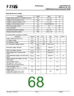
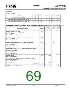
Preliminary
VG37648041AT
256M:x4, x8, x16
VIS
CMOS Synchronous Dynamic RAM
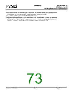
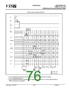
NOTES
1. All voltages referenced to Vss.
2. Tests for AC timing, IDD, and electrical, AC and DC characteristics, may be conducted at nominal refer-
ence/supply voltage levels, but the related specifications and device operation are guaranteed for the full
voltage range specified.
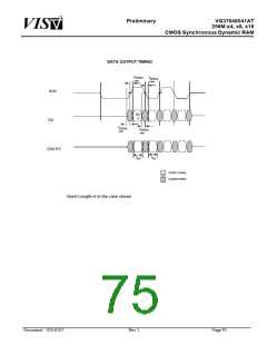
3. Outputs measured with equivalent load:
VTT
W
25
W
25
Output
(VOUT)
(Test point)
30pF
4.AC timing and IDD tests may use a V to V swing of up to 1.5V in the test environment, but input timing is
IL
IH
still referenced to V
(or to the crossing point for CLK/CLK#), and parameter specifications are guaran-
REF
teed for the specified AC input levels under normal use conditions. The minimum slew rate for the input sig-
nals used to test the device is 1V/ns in the range between V and V
.
IH(AC)
IL(AC)
5.The AC and DC input level specifications are as defined in the SSTL_2 Standard (i.e. the receiver will effec-
tively switch as a result of the signal crossing the AC input level, and will remain in that state as long as the
signal does not ring back above (below) the DC input LOW(HIGH) level.
6.V
is expected to track variations in the DC level of V
of the transmitting device. peak-to-peak noise
DDQ
REF
on V
may not exceed +/-2% of the DC value.
REF
7.VTT is not applied directly to the device. VTT is a system supply for signal termination resistors, is expected
to be set equal to V and must track variations in the DC level of V
.
REF
REF
8.VID is the magnitude of the difference between the input level on CLK and the input level on CLK#.
9.The value of V is expected to equal V and must track variations in the DC level of V
.
REF
IX
REF
10.IDD is dependent on output loading and cycle rates.
Specified values are obtained with minimum cycle time and the outputs open.
11.Enables on chip refresh and address counters.
12.IDD specifications are tested after the device is properly initialized.
t
13.This parameter is sampled. VDDQ+2.5V ±0.2V , VDD=+3.3V±3.3V , f=1MHz, A=25°C
14.Input slew rate=1V/ns+/-20%.
15.The CLK/CLK# input reference level (for timeing referenced to CLK/CLK#) is the point at which CLK and
CLK# cross; the input reference level for signals other than CLK/CLK#, is VREF.
16.Inputs are not recognized as valid until V
stabilizes. Exceptions: during the period before V
stabi
REF
REF
lizes, CKE=<0.3V
is recognized as LOW.
DDQ
17.The output timing reference level, as measured at the test point indicated in Note 3, is V
.
TT
t
t
18. HZ and LZ transitions occur in the same access time windows as valid data transitions. These parame-
ters are not referenced to a specific voltage level, but specify when the device output is no longer driving
(HZ), or begins driving (LZ).
19.The maximum limit for this parameter is not a device limit. The device will operate with a greater value for
this parameter, but system performance (bus turnaround) will degrade accordingly.
Document : 1G5-0157
Rev.1
Page72

 VML [ VANGUARD INTERNATIONAL SEMICONDUCTOR ]