Preliminary
VG37648041AT
256M:x4, x8, x16
VIS
CMOS Synchronous Dynamic RAM
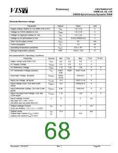
Absolute Maximum ratings
Paramefer
Sysbol
VDD
Value
Unit
V
Supply voltage relative to Vss (With VDD 3.3V)
-1.0 + 4.6
Voltage on VDDQ relative to Vss
Voltage on input pin relative to Vss
Voltage on I/O pin relative to Vss
Short circuit output current
VDDQ
VIN
-1.0 + 3.6
-1.0 + 3.6
-0.5 to VDDQ+0.5
50
V
V
VI/O
V
VOUT
PD
mA
W
°C
°C
Power dissipation
1.0
Operating temperature (ambient)
Storage temperature (plastic)
TOPT
PRE
0 to + 70
-55 to + 125
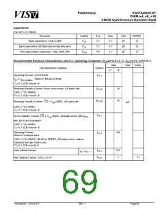
Recommended DC Operating Conditions
Typ
Unit
V
Notes
Parameter
Symbol
Min
Max
Supply voltage (with VDD 3.3V)
VDD
VDDQ
VREF
VTT
3.6
2.7
3.0
2.3
3.3
2.5
I/O Supply Voltage
V
I/O Reference Voltage
1.15
1.25
1.35
V
6
7
I/O Termination Voltage (system)
VREF-
0.04
VREF
VREF+0.04
V
Input high Voltage, all inputs
Input Low voltage, all inputs
VIH(DC)
VREF
+0.18
-
VDD+0.3
V
VIL(DC)
VIN(DC)
-0.3
-0.3
-
-
VREF-0.18
VDDQ+0.3
V
V
Input Voltage Level. CLK and CLK#
inputs
Input Differential Voltage, CLK and CLK#
inputs
VID(DC)
VIX(DC)
II
0.36
1.15
-5
-
-
-
VDD+0.6
V
V
8
9
Input Crossing Point Voltage, CLK and
CLK# inputs
1.35
5
Input Leakage Current
uA
Any input 0V ³ VIN £ VDD
(All other pins not under test=0V)
Output Leakage Current
IOZ
-5
-
-
5
uA
(DQs are disbled; ) 0V ³ VOUT £ VDDQ
Output Levels
Output High Current (Vout=1.95V)
IOH
IOL
-15.2
-
mA
15.2
Output Low current (Vout=0.35V)
Document : 1G5-0157
Rev.1
Page68

 VML [ VANGUARD INTERNATIONAL SEMICONDUCTOR ]