Preliminary
VG37648041AT
256M:x4, x8, x16
VIS
CMOS Synchronous Dynamic RAM
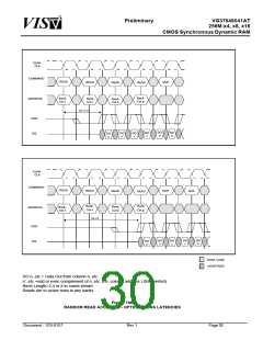
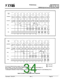
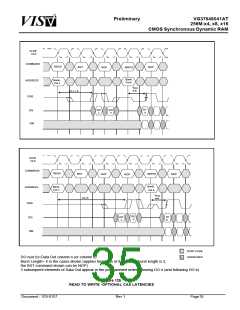
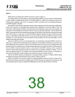
CLK#
CLK
COMMAND
READ
BST
NOP
NOP
NOP
WRITE
Bank,
Col b
Bank,
Col n
ADDRESS
DQS
tDSS
min
CL=2
D1
b
DO
n
DQ
DM
DO
n’
CLK#
CLK
COMMAND
READ
BST
WRITE
NOP
NOP
NOP
Bank,
Col b
Bank,
Col n
ADDRESS
DQS
tDSS
min
CL=2.5
DO
DO
n’
n
D1
b
DQ
DM
DONT’ CARE
UNDEFINED
DO n(or b)=Data Out from column n (or column b)
Burst Length= 4 in the cases shown (applies for bursts of 8 as well; if burst length is 2,
the BST command shown can be NOP)
3 subsequent elements of Data Out appear in the programmed order following DO n (and following DO b)
Figure 12a
READ TO WRITE - REQUIRED CAS LATENCIES
Document : 1G5-0157
Rev.1
Page34

 VML [ VANGUARD INTERNATIONAL SEMICONDUCTOR ]