Preliminary
VG37648041AT
256M:x4, x8, x16
VIS
CMOS Synchronous Dynamic RAM
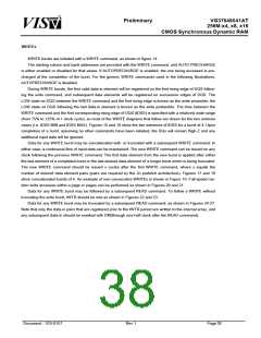
WRITEs
WRITE bursts are initiated with a WRITE command, as shown in figure 14.
The starting column and bank addresses are provided with the WRITE command, and AUTO PRECHARGE
is either enabled or disabled for that acess. If AUTOPRECHARGE is enabled, the row being accessed is pre-
charged at the completion of the burst. For the generic WRITE commands used in the following illustrations,
AUTOPRECHARGE is disabled.
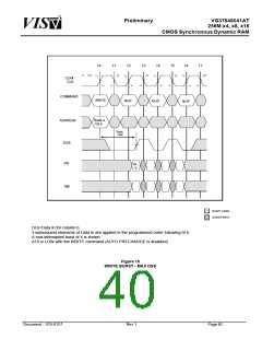
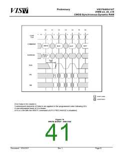
During WRITE bursts, the first valid data-in element will be registered on the first rising edge of DQS follow-
ing the write command, and subsequent data elements will be registered on successive edges of DQS. The
LOW state on DQS between the WRITE command and the first rising edge is known as the write preamble; the
LOW state on DQS following the last data-in element is known as the write postamble. The time between the
WRITE command and the first corresponding rising edge of DQS (tDSS) is specified with a relatively wide range
(from 75% to 125% of 1 clock cycle), so most of the WRITE diagrams that follow are drawn for the two extreme
cases (i.e. tDSS MIN and tDSS MAX). Figures 15 and 16 show the two extremes of tDSS for a burst of 4. Upon
completion of a burst, assuming no other commands have been initiated, the DQs will remain High-Z and any
additional input data will be ignored.
Data for any WRITE burst may be concatenated with or truncated with a subsequent WRITE command. In
either case, a continuous flow of input data can be maintained. The new WRITE command can be issued on any
clock following the previous WRITE command. The first data element from the new burst is applied after either
the last element of a completed burst or the last desired data element of a longer burst which is being truncated.
The new WRITE command should be issued x cycles after the first WRITE command, where x equals the
number of desired data element pairs (pairs are required by the 2n prefetch architecture). Figures 17 and 18
show concatenated bursts of 4. An example of non-consecutive WRITEs is shown in Figure 19. Full-speed ran-
dom write accesses within a page or pages can be performed as shown in Figures 20 and 21.
Data for any WRITE burst may be followed by a subsequent READ command. To follow a WRITE without
truncating the write burst, tWTR should be met as shown in Figures 22 and 23.
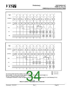
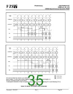
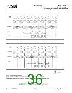
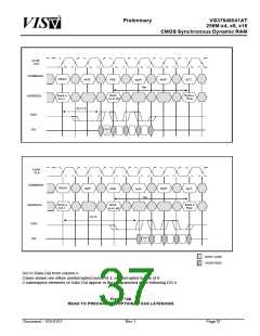
Data for any WRITE burst may be truncated by a subsequent READ command, as shown in Figures 24-27.
Note that only the data-in pairs that are registered prior to the tWTR period are written to the internal array, and
any subsequent data-in should be masked with DM(through one-half clock after the READ command).
Document : 1G5-0157
Rev.1
Page38

 VML [ VANGUARD INTERNATIONAL SEMICONDUCTOR ]