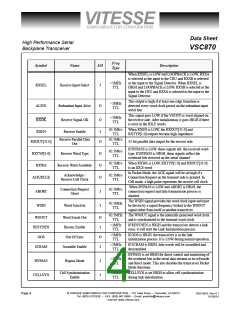
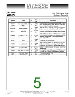
VITESSE
SEMICONDUCTOR CORPORATION
Data Sheet
High Performance Serial
Backplane Transceiver
VSC870
1.1.5 Cell Synchronization
If the CELLSYN signal is set HIGH, after the word synchronization process, the transceiver starts the cell
synchronization process. In this process, the transceiver detects the received cell clock sent from the switch. The cell
clock is embedded in the command words with overhead bits ‘00’ as described in section 3.2. The received cell clock
is output on ACK/RCLK. The switch chip connects each port to itself after link initialization. By sending a special
ALIGN word to itself, the transceiver can adjust the transmit cell clock (RTM/TCLK) until it is properly phase
shifted relative to the received cell clock. If cells are sent from the transceiver aligned to this transmit cell clock, they
will arrive at the switch aligned to the master cell clock which is originated at the switch. The received cell clock on
the serial link is therefore shifted by N word clocks to create a phase shifted cell clock which is output on RTM/
TCLK. An on-chip counter provides this phase shift, with the frequency and phase shift determined during the cell
synchronization process. For this alignment process to work, the minimum cell size is 13 words (52 bytes).
1.1.6 Cell Synchronization for Multiple Transceivers
If two or more transceivers are used in parallel on a port card in order to increase bandwidth, skew between
signals could cause the transmit cell clock (RTM/TCLK) in one or more transceivers to be shifted in phase by one
word clock relative to the other transceivers. To adjust out this offset, a marker cell clock can be sent to both
transceivers. This is done by sending the signal RTM/TCLK from the master transceiver to the DLYEN/CCKIN input
on the slave transceivers. At the end of the cell synchronization process, the pipeline offset is adjusted out using this
marker cell clock. See Application Note 32 for more details.
1.1.7 Link Error Detection
Receive errors are declared if the transceiver detects a bit pattern error in an IDLE word in the received serial
data by generating a HIGH pulse on RXOK. In cell mode, if an IDLE word is received at the end of the cell period
and it does not contain the embedded cell clock, or it receives an embedded cell clock at the wrong time, it generates
a HIGH pulse on TXOK. This error is stored internally and if the RESYNEN goes HIGH, the VSC870 will start the
link initialization process. The RXOK and TXOK signals can therefore be tied to the RESYNEN signal to start the
link initialization process immediately, or the user logic can monitor the RXOK and TXOK signals when OOS is
LOW and assert RESYNEN only after an error threshold has been reached. It is up to the user to make sure enough
IDLE words are used to detect errors during system operation. The switch can initiate the initialization process by
forcing zeroes on the serial link. If the transceiver receives 4 consecutive words of all zeroes, it will immediately start
the initialization process.
1.2 Data Encoding Format
To provide self routing and signalling functions, the transceiver and switch require different data types to
differentiate between data words, connection request words or command words. Depending on the mode that the
transceiver is in, different data types are recognized at the transceiver parallel interface. These word types are
encoded using the RXTYP[1:0] or TXTYP[1:0] bits. At the transceiver to switch serial interface, these data types are
encoded in the two overhead bits (B[1:0]). Sections 2.2, 3.2 and 4.2 describe these data types in more detail.
The format for data words and command words the transceiver parallel interfaces and on the serial data lines
between the transceiver and switch chip are described in the following sections. The format for the connection
request word is described later in the Packet Mode section.
© VITESSE SEMICONDUCTOR CORPORATION • 741 Calle Plano • Camarillo, CA 93012
Tel: (800) VITESSE • FAX: (805) 987-5896 • Email: prodinfo@vitesse.com
Internet: www.vitesse.com
Page 8
G52190-0, Rev 4.1
01/05/01

 VITESSE [ VITESSE SEMICONDUCTOR CORPORATION ]